

In this Verilog project, Verilog code for a 16-bit RISC processor is presented.
The RISC processor is designed based on its instruction set and Harvard-type data path structure. Then, the RISC processor is implemented in Verilog and verified using Xilinx ISIM.

The instruction set of the RISC processor:
A. Memory Access Instructions
1. Load Word:
LD ws, offset(rs1) ws:=Mem16[rs1 + offset]
2. Store Word:
2. Store Word:
ST rs2, offset(rs1) Mem16[rs1 + offset]=rs2
B. Data Processing Instructions
1. Add:
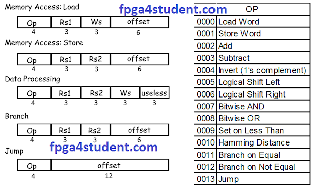
B. Data Processing Instructions
1. Add:
ADD ws, rs1, rs2 ws:=rs1 + rs2
2. Subtract:
2. Subtract:
SUB ws, rs1, rs2 ws:=rs1 – rs2
3. Invert (1‘s complement):
3. Invert (1‘s complement):
INV ws, rs1 ws:=!rs1
4. Logical Shift Left:
4. Logical Shift Left:
LSL ws, rs1, rs2 ws:=rs1 << rs2
5. Logical Shift Right:
5. Logical Shift Right:
LSR ws, rs1, rs2 ws:=rs1 >> rs2
6. Bitwise AND:
6. Bitwise AND:
AND ws, rs1, rs2 ws:=rs1 • rs2
7. Bitwise OR:
7. Bitwise OR:
OR ws, rs1, rs2 ws:=rs1 | rs2
8. Set on Less Than:
SLT ws, rs1, rs2 ws:=1 if rs1 < rs2; ws:=0 if rs1 ≥ rs2
C. Control Flow Instructions
1. Branch on Equal:
BEQ rs1, rs2, offset
Branch to (PC + 2 + (offset << 1)) when rs1 = rs2
2. Branch on Not Equal:
BNE rs1, rs2, offset
Branch to (PC + 2 + (offset << 1)) when rs1 != rs2
3. Jump: JMP offset Jump to {PC [15:13], (offset << 1)}
Instruction Format of the RISC processor :
Processor Control Unit Design:
Control signals
| |||||||||
Instruction
|
Reg
Dst
|
ALUSrc
|
Memto
Reg
|
Reg
Write
|
MemRead
|
Mem
Write
|
Branch
|
ALUOp
|
Jump
|
Data-processing
|
1
|
0
|
0
|
1
|
0
|
0
|
0
|
00
|
0
|
LW
|
0
|
1
|
1
|
1
|
1
|
0
|
0
|
10
|
0
|
SW
|
0
|
1
|
0
|
0
|
0
|
1
|
0
|
10
|
0
|
BEQ,BNE
|
0
|
0
|
0
|
0
|
0
|
0
|
1
|
01
|
0
|
J
|
0
|
0
|
0
|
0
|
0
|
0
|
0
|
00
|
1
|
ALU Control Unit Design:
ALU Control
| ||||
ALUOp
|
Opcode(hex)
|
ALUcnt
|
ALU Operation
|
Instruction
|
10
|
xxxx
|
000
|
ADD
|
LW,SW
|
01
|
xxxx
|
001
|
SUB
|
BEQ,BNE
|
00
|
0002
|
000
|
ADD
|
D-type: ADD
|
00
|
0003
|
001
|
SUB
|
D-type: SUB
|
00
|
0004
|
010
|
INVERT
|
D-type: INVERT
|
00
|
0005
|
011
|
LSL
|
D-type: LSL
|
00
|
0006
|
100
|
LSR
|
D-type: LSR
|
00
|
0007
|
101
|
AND
|
D-type: AND
|
00
|
0008
|
110
|
OR
|
D-type: OR
|
00
|
0009
|
111
|
SLT
|
D-type: SLT
|
Verilog code for the RISC processor:
1. Verilog code for Instruction Memory :
`include "Parameter.v"
// fpga4student.com
// FPGA projects, VHDL projects, Verilog projects
// Verilog code for RISC Processor
// Verilog code for Instruction Memory
module Instruction_Memory(
 input[15:0] pc,
 output[15:0] instruction
);

 reg [`col - 1:0] memory [`row_i - 1:0];
 wire [3 : 0] rom_addr = pc[4 : 1];
 initial
 begin
  $readmemb("./test/test.prog", memory,0,14);
 end
 assign instruction =  memory[rom_addr];

endmodule
2. Verilog code for register file:
`timescale 1ns / 1ps
// fpga4student.com
// FPGA projects, VHDL projects, Verilog projects
// Verilog code for RISC Processor
// Verilog code for register file
module GPRs(
 input    clk,
 // write port
 input    reg_write_en,
 input  [2:0] reg_write_dest,
 input  [15:0] reg_write_data,
 //read port 1
 input  [2:0] reg_read_addr_1,
 output  [15:0] reg_read_data_1,
 //read port 2
 input  [2:0] reg_read_addr_2,
 output  [15:0] reg_read_data_2
);
 reg [15:0] reg_array [7:0];
 integer i;
 // write port
 //reg [2:0] i;
 initial begin
  for(i=0;i<8;i=i+1)
   reg_array[i] <= 16'd0;
 end
 always @ (posedge clk ) begin
   if(reg_write_en) begin
    reg_array[reg_write_dest] <= reg_write_data;
   end
 end


 assign reg_read_data_1 = reg_array[reg_read_addr_1];
 assign reg_read_data_2 = reg_array[reg_read_addr_2];


endmodule
3. Verilog code for Data Memory:
`include "Parameter.v" // fpga4student.com // FPGA projects, VHDL projects, Verilog projects // Verilog code for RISC Processor // Verilog code for data Memory module Data_Memory( input clk, // address input, shared by read and write port input [15:0] mem_access_addr, // write port input [15:0] mem_write_data, input mem_write_en, input mem_read, // read port output [15:0] mem_read_data ); reg [`col - 1:0] memory [`row_d - 1:0]; integer f; wire [2:0] ram_addr=mem_access_addr[2:0]; initial begin $readmemb("./test/test.data", memory); f = $fopen(`filename); $fmonitor(f, "time = %d\n", $time, "\tmemory[0] = %b\n", memory[0], "\tmemory[1] = %b\n", memory[1], "\tmemory[2] = %b\n", memory[2], "\tmemory[3] = %b\n", memory[3], "\tmemory[4] = %b\n", memory[4], "\tmemory[5] = %b\n", memory[5], "\tmemory[6] = %b\n", memory[6], "\tmemory[7] = %b\n", memory[7]); `simulation_time; $fclose(f); end always @(posedge clk) begin if (mem_write_en) memory[ram_addr] <= mem_write_data; end assign mem_read_data = (mem_read==1'b1) ? memory[ram_addr]: 16'd0;endmodule
4. Verilog code for ALU unit:
// fpga4student.com
// FPGA projects, VHDL projects, Verilog projects
// Verilog code for RISC Processor
// Verilog code for ALU
module ALU(
 input  [15:0] a,  //src1
 input  [15:0] b,  //src2
 input  [2:0] alu_control, //function sel

 output reg [15:0] result,  //result
 output zero
    );

always @(*)
begin
 case(alu_control)
 3'b000: result = a + b; // add
 3'b001: result = a - b; // sub
 3'b010: result = ~a;
 3'b011: result = a<<b;
 3'b100: result = a>>b;
 3'b101: result = a & b; // and
 3'b110: result = a | b; // or
 3'b111: begin if (a<b) result = 16'd1;
    else result = 16'd0;
    end
 default:result = a + b; // add
 endcase
end
assign zero = (result==16'd0) ? 1'b1: 1'b0;

endmodule
5. Verilog code for ALU Control Unit of the RISC processor:
`timescale 1ns / 1ps
//fpga4student.com: FPGA projects, Verilog projects, VHDL projects
// Verilog code for 16-bit RISC processor
// ALU_Control Verilog code
module alu_control( ALU_Cnt, ALUOp, Opcode);
 output reg[2:0] ALU_Cnt;
 input [1:0] ALUOp;
 input [3:0] Opcode;
 wire [5:0] ALUControlIn;
 assign ALUControlIn = {ALUOp,Opcode};
 always @(ALUControlIn)
 casex (ALUControlIn)
   6'b10xxxx: ALU_Cnt=3'b000;
   6'b01xxxx: ALU_Cnt=3'b001;
   6'b000010: ALU_Cnt=3'b000;
   6'b000011: ALU_Cnt=3'b001;
   6'b000100: ALU_Cnt=3'b010;
   6'b000101: ALU_Cnt=3'b011;
   6'b000110: ALU_Cnt=3'b100;
   6'b000111: ALU_Cnt=3'b101;
   6'b001000: ALU_Cnt=3'b110;
   6'b001001: ALU_Cnt=3'b111;
  default: ALU_Cnt=3'b000;
  endcase
endmodule
6. Verilog code for Datapath of the RISC processor:
`timescale 1ns / 1ps
// fpga4student.com
// FPGA projects, VHDL projects, Verilog projects
// Verilog code for RISC Processor
// Verilog code for Data Path of the processor
module Datapath_Unit(
 input clk,
 input jump,beq,mem_read,mem_write,alu_src,reg_dst,mem_to_reg,reg_write,bne,
 input[1:0] alu_op,
 output[3:0] opcode
);
 reg  [15:0] pc_current;
 wire [15:0] pc_next,pc2;
 wire [15:0] instr;
 wire [2:0] reg_write_dest;
 wire [15:0] reg_write_data;
 wire [2:0] reg_read_addr_1;
 wire [15:0] reg_read_data_1;
 wire [2:0] reg_read_addr_2;
 wire [15:0] reg_read_data_2;
 wire [15:0] ext_im,read_data2;
 wire [2:0] ALU_Control;
 wire [15:0] ALU_out;
 wire zero_flag;
 wire [15:0] PC_j, PC_beq, PC_2beq,PC_2bne,PC_bne;
 wire beq_control;
 wire [12:0] jump_shift;
 wire [15:0] mem_read_data;
 // PC
 initial begin
  pc_current <= 16'd0;
 end
 always @(posedge clk)
 begin
   pc_current <= pc_next;
 end
 assign pc2 = pc_current + 16'd2;
 // instruction memory
 Instruction_Memory im(.pc(pc_current),.instruction(instr));
 // jump shift left 2
 assign jump_shift = {instr[11:0],1'b0};
 // multiplexer regdest
 assign reg_write_dest = (reg_dst==1'b1) ? instr[5:3] :instr[8:6];
 // register file
 assign reg_read_addr_1 = instr[11:9];
 assign reg_read_addr_2 = instr[8:6];

 // GENERAL PURPOSE REGISTERs
 GPRs reg_file
 (
  .clk(clk),
  .reg_write_en(reg_write),
  .reg_write_dest(reg_write_dest),
  .reg_write_data(reg_write_data),
  .reg_read_addr_1(reg_read_addr_1),
  .reg_read_data_1(reg_read_data_1),
  .reg_read_addr_2(reg_read_addr_2),
  .reg_read_data_2(reg_read_data_2)
 );
 // immediate extend
 assign ext_im = {{10{instr[5]}},instr[5:0]};
 // ALU control unit
 alu_control ALU_Control_unit(.ALUOp(alu_op),.Opcode(instr[15:12]),.ALU_Cnt(ALU_Control));
 // multiplexer alu_src
 assign read_data2 = (alu_src==1'b1) ? ext_im : reg_read_data_2;
 // ALU
 ALU alu_unit(.a(reg_read_data_1),.b(read_data2),.alu_control(ALU_Control),.result(ALU_out),.zero(zero_flag));
 // PC beq add
 assign PC_beq = pc2 + {ext_im[14:0],1'b0};
 assign PC_bne = pc2 + {ext_im[14:0],1'b0};
 // beq control
 assign beq_control = beq & zero_flag;
 assign bne_control = bne & (~zero_flag);
 // PC_beq
 assign PC_2beq = (beq_control==1'b1) ? PC_beq : pc2;
 // PC_bne
 assign PC_2bne = (bne_control==1'b1) ? PC_bne : PC_2beq;
 // PC_j
 assign PC_j = {pc2[15:13],jump_shift};
 // PC_next
 assign pc_next = (jump == 1'b1) ? PC_j :  PC_2bne;

 /// Data memory
  Data_Memory dm
   (
    .clk(clk),
    .mem_access_addr(ALU_out),
    .mem_write_data(reg_read_data_2),
    .mem_write_en(mem_write),
    .mem_read(mem_read),
    .mem_read_data(mem_read_data)
   );

 // write back
 assign reg_write_data = (mem_to_reg == 1'b1)?  mem_read_data: ALU_out;
 // output to control unit
 assign opcode = instr[15:12];
endmodule
7. Verilog code for the Control Unit of the RISC processor:
`timescale 1ns / 1ps
// fpga4student.com
// FPGA projects, VHDL projects, Verilog projects
// Verilog code for RISC Processor
// Verilog code for Control Unit
module Control_Unit(
      input[3:0] opcode,
      output reg[1:0] alu_op,
      output reg jump,beq,bne,mem_read,mem_write,alu_src,reg_dst,mem_to_reg,reg_write
    );


always @(*)
begin
 case(opcode)
 4'b0000:  // LW
   begin
    reg_dst = 1'b0;
    alu_src = 1'b1;
    mem_to_reg = 1'b1;
    reg_write = 1'b1;
    mem_read = 1'b1;
    mem_write = 1'b0;
    beq = 1'b0;
    bne = 1'b0;
    alu_op = 2'b10;
    jump = 1'b0;
   end
 4'b0001:  // SW
   begin
    reg_dst = 1'b0;
    alu_src = 1'b1;
    mem_to_reg = 1'b0;
    reg_write = 1'b0;
    mem_read = 1'b0;
    mem_write = 1'b1;
    beq = 1'b0;
    bne = 1'b0;
    alu_op = 2'b10;
    jump = 1'b0;
   end
 4'b0010:  // data_processing
   begin
    reg_dst = 1'b1;
    alu_src = 1'b0;
    mem_to_reg = 1'b0;
    reg_write = 1'b1;
    mem_read = 1'b0;
    mem_write = 1'b0;
    beq = 1'b0;
    bne = 1'b0;
    alu_op = 2'b00;
    jump = 1'b0;
   end
 4'b0011:  // data_processing
   begin
    reg_dst = 1'b1;
    alu_src = 1'b0;
    mem_to_reg = 1'b0;
    reg_write = 1'b1;
    mem_read = 1'b0;
    mem_write = 1'b0;
    beq = 1'b0;
    bne = 1'b0;
    alu_op = 2'b00;
    jump = 1'b0;
   end
 4'b0100:  // data_processing
   begin
    reg_dst = 1'b1;
    alu_src = 1'b0;
    mem_to_reg = 1'b0;
    reg_write = 1'b1;
    mem_read = 1'b0;
    mem_write = 1'b0;
    beq = 1'b0;
    bne = 1'b0;
    alu_op = 2'b00;
    jump = 1'b0;
   end
 4'b0101:  // data_processing
   begin
    reg_dst = 1'b1;
    alu_src = 1'b0;
    mem_to_reg = 1'b0;
    reg_write = 1'b1;
    mem_read = 1'b0;
    mem_write = 1'b0;
    beq = 1'b0;
    bne = 1'b0;
    alu_op = 2'b00;
    jump = 1'b0;
   end
 4'b0110:  // data_processing
   begin
    reg_dst = 1'b1;
    alu_src = 1'b0;
    mem_to_reg = 1'b0;
    reg_write = 1'b1;
    mem_read = 1'b0;
    mem_write = 1'b0;
    beq = 1'b0;
    bne = 1'b0;
    alu_op = 2'b00;
    jump = 1'b0;
   end
 4'b0111:  // data_processing
   begin
    reg_dst = 1'b1;
    alu_src = 1'b0;
    mem_to_reg = 1'b0;
    reg_write = 1'b1;
    mem_read = 1'b0;
    mem_write = 1'b0;
    beq = 1'b0;
    bne = 1'b0;
    alu_op = 2'b00;
    jump = 1'b0;
   end
 4'b1000:  // data_processing
   begin
    reg_dst = 1'b1;
    alu_src = 1'b0;
    mem_to_reg = 1'b0;
    reg_write = 1'b1;
    mem_read = 1'b0;
    mem_write = 1'b0;
    beq = 1'b0;
    bne = 1'b0;
    alu_op = 2'b00;
    jump = 1'b0;
   end
 4'b1001:  // data_processing
   begin
    reg_dst = 1'b1;
    alu_src = 1'b0;
    mem_to_reg = 1'b0;
    reg_write = 1'b1;
    mem_read = 1'b0;
    mem_write = 1'b0;
    beq = 1'b0;
    bne = 1'b0;
    alu_op = 2'b00;
    jump = 1'b0;
   end
 4'b1011:  // BEQ
   begin
    reg_dst = 1'b0;
    alu_src = 1'b0;
    mem_to_reg = 1'b0;
    reg_write = 1'b0;
    mem_read = 1'b0;
    mem_write = 1'b0;
    beq = 1'b1;
    bne = 1'b0;
    alu_op = 2'b01;
    jump = 1'b0;
   end
 4'b1100:  // BNE
   begin
    reg_dst = 1'b0;
    alu_src = 1'b0;
    mem_to_reg = 1'b0;
    reg_write = 1'b0;
    mem_read = 1'b0;
    mem_write = 1'b0;
    beq = 1'b0;
    bne = 1'b1;
    alu_op = 2'b01;
    jump = 1'b0;
   end
 4'b1101:  // J
   begin
    reg_dst = 1'b0;
    alu_src = 1'b0;
    mem_to_reg = 1'b0;
    reg_write = 1'b0;
    mem_read = 1'b0;
    mem_write = 1'b0;
    beq = 1'b0;
    bne = 1'b0;
    alu_op = 2'b00;
    jump = 1'b1;
   end
 default: begin
    reg_dst = 1'b1;
    alu_src = 1'b0;
    mem_to_reg = 1'b0;
    reg_write = 1'b1;
    mem_read = 1'b0;
    mem_write = 1'b0;
    beq = 1'b0;
    bne = 1'b0;
    alu_op = 2'b00;
    jump = 1'b0;
   end
 endcase
 end

endmodule
8. Verilog code for the 16-bit RISC processor:
`timescale 1ns / 1ps
// fpga4student.com
// FPGA projects, VHDL projects, Verilog projects
// Verilog code for RISC Processor

module Risc_16_bit(
 input clk
);
 wire jump,bne,beq,mem_read,mem_write,alu_src,reg_dst,mem_to_reg,reg_write;
 wire[1:0] alu_op;
 wire [3:0] opcode;
 // Datapath
 Datapath_Unit DU
 (
  .clk(clk),
  .jump(jump),
  .beq(beq),
  .mem_read(mem_read),
  .mem_write(mem_write),
  .alu_src(alu_src),
  .reg_dst(reg_dst),
  .mem_to_reg(mem_to_reg),
  .reg_write(reg_write),
  .bne(bne),
  .alu_op(alu_op),
  .opcode(opcode)
 );
 // control unit
 Control_Unit control
 (
  .opcode(opcode),
  .reg_dst(reg_dst),
  .mem_to_reg(mem_to_reg),
  .alu_op(alu_op),
  .jump(jump),
  .bne(bne),
  .beq(beq),
  .mem_read(mem_read),
  .mem_write(mem_write),
  .alu_src(alu_src),
  .reg_write(reg_write)
 );

endmodule
9. Verilog Testbench code for the 16-bit RISC Processor:
`timescale 1ns / 1ps
`include "Parameter.v"
// fpga4student.com
// FPGA projects, VHDL projects, Verilog projects
// Verilog code for RISC Processor
// Verilog testbench code to test the processor
module test_Risc_16_bit;

 // Inputs
 reg clk;

 // Instantiate the Unit Under Test (UUT)
 Risc_16_bit uut (
  .clk(clk)
 );

 initial
  begin
   clk <=0;
   `simulation_time;
   $finish;
  end

 always
  begin
   #5 clk = ~clk;
  end

endmodule
Parameter file:
`ifndef PARAMETER_H_
`define PARAMETER_H_
// fpga4student.com
// FPGA projects, VHDL projects, Verilog projects
// Verilog code for RISC Processor
// Parameter file
`define col 16 // 16 bits instruction memory, data memory
`define row_i 15 // instruction memory, instructions number, this number can be changed. Adding more instructions to verify your design is a good idea.
`define row_d 8 // The number of data in data memory. We only use 8 data. Do not change this number. You can change the value of each data inside test.data file. Total number is fixed at 8.
`define filename "./test/50001111_50001212.o"
`define simulation_time #160

`endif
All Verilog code needed for the 16-bit RISC processor are provided. Now, you just need to create a test.data (Initial content of data memory) and test.prog (Intruction memory). Then, run simulation to see how the process works on simulation waveform and memory files.
Example instruction memory file:
0000_0100_0000_0000 // load R0 <- Mem(R2 + 0)
0000_0100_0100_0001 // load R1 <- Mem(R2 + 1)
0010_0000_0101_0000 // Add R2 <- R0 + R1
0001_0010_1000_0000 // Store Mem(R1 + 0) <- R2
0011_0000_0101_0000 // sub R2 <- R0 - R1
0100_0000_0101_0000 // invert R2 <- !R0
0101_0000_0101_0000 // logical shift left R2 <- R0<<R1
0110_0000_0101_0000 // logical shift right R2 <- R0>>R1
0111_0000_0101_0000 // AND R2<- R0 AND R1
1000_0000_0101_0000 // OR R2<- R0 OR R1
1001_0000_0101_0000 // SLT R2 <- 1 if R0 < R1
0010_0000_0000_0000 // Add R0 <- R0 + R0
1011_0000_0100_0001 // BEQ branch to jump if R0=R1, PCnew= PC+2+offset<<1 = 28 => offset = 1
1100_0000_0100_0000 // BNE branch to jump if R0!=R1, PCnew= PC+2+offset<<1 = 28 => offset = 0
1101_0000_0000_0000 // J jump to the beginning address
Example data memory file:
0000_0000_0000_0001
0000_0000_0000_0010
0000_0000_0000_0001
0000_0000_0000_0010
0000_0000_0000_0001
0000_0000_0000_0010
0000_0000_0000_0001
0000_0000_0000_0010
You may like this:
MIPS Processor in VHDL
Verilog code for 16-bit single-cycle MIPS processor
32-bit 5-stage Pipelined MIPS Processor in Verilog (Part-1)
32-bit 5-stage Pipelined MIPS Processor in Verilog (Part-2)
32-bit 5-stage Pipelined MIPS Processor in Verilog (Part-3)
29. Verilog code for Multiplexers
30. N-bit Adder Design in Verilog
31. Verilog vs VHDL: Explain by Examples
32. Verilog code for Clock divider on FPGA
33. How to generate a clock enable signal in Verilog
34. Verilog code for PWM Generator
35. Verilog coding vs Software Programming
36. Verilog code for Moore FSM Sequence Detector
37. Verilog code for 7-segment display controller on Basys 3 FPGA
MIPS Processor in VHDL
Verilog code for 16-bit single-cycle MIPS processor
32-bit 5-stage Pipelined MIPS Processor in Verilog (Part-1)
32-bit 5-stage Pipelined MIPS Processor in Verilog (Part-2)
32-bit 5-stage Pipelined MIPS Processor in Verilog (Part-3)
Recommended Verilog projects:
2. Verilog code for FIFO memory
3. Verilog code for 16-bit single-cycle MIPS processor
4. Programmable Digital Delay Timer in Verilog HDL
5. Verilog code for basic logic components in digital circuits
6. Verilog code for 32-bit Unsigned Divider
7. Verilog code for Fixed-Point Matrix Multiplication
8. Plate License Recognition in Verilog HDL
9. Verilog code for Carry-Look-Ahead Multiplier
10. Verilog code for a Microcontroller
11. Verilog code for 4x4 Multiplier
12. Verilog code for Car Parking System
13. Image processing on FPGA using Verilog HDL
14. How to load a text file into FPGA using Verilog HDL
15. Verilog code for Traffic Light Controller
16. Verilog code for Alarm Clock on FPGA
17. Verilog code for comparator design
18. Verilog code for D Flip Flop
19. Verilog code for Full Adder
20. Verilog code for counter with testbench
21. Verilog code for 16-bit RISC Processor
22. Verilog code for button debouncing on FPGA
23. How to write Verilog Testbench for bidirectional/ inout ports
24. Tic Tac Toe Game in Verilog and LogiSim
25. 32-bit 5-stage Pipelined MIPS Processor in Verilog (Part-1)
26. 32-bit 5-stage Pipelined MIPS Processor in Verilog (Part-2)
27. 32-bit 5-stage Pipelined MIPS Processor in Verilog (Part-3)
28. Verilog code for Decoder25. 32-bit 5-stage Pipelined MIPS Processor in Verilog (Part-1)
26. 32-bit 5-stage Pipelined MIPS Processor in Verilog (Part-2)
27. 32-bit 5-stage Pipelined MIPS Processor in Verilog (Part-3)
29. Verilog code for Multiplexers
30. N-bit Adder Design in Verilog
31. Verilog vs VHDL: Explain by Examples
32. Verilog code for Clock divider on FPGA
33. How to generate a clock enable signal in Verilog
34. Verilog code for PWM Generator
35. Verilog coding vs Software Programming
36. Verilog code for Moore FSM Sequence Detector
37. Verilog code for 7-segment display controller on Basys 3 FPGA


ALU_Control_unit module is missing !
ReplyDeleteUpdated. Thanks.
DeleteDescription of ALU and ALU Control is still missing in the Datapath.
ReplyDeleteCheck the given table to understand the functionality of ALU and ALU control unit.
ReplyDeleteto implent it on fpga module like spartan,can you please give a heads up
ReplyDeletecan yo just explain about the test.prog and test.data ,where should we create it and also about the .o file.
ReplyDeleteThanks in advance.
These files were given above. Just create the file with the same names and copy the contents into these files.
Deletecan u pls send me this code
ReplyDeletemy mail is
manju.upadhya17@gmail.com
Can u send 8bit RISC processor code??
ReplyDeleteThank you for the above code. I tested it , works perfectly. I got an overview now. Thanks again.
ReplyDeleteGlad to hear that. You're welcome.
DeleteCan you please send the codes beacuse i have tested and it was showing some errors the tool i have used is xilinx 14.3 version and still not showing the output
Deletehow to create a test.data (Initial content of data memory) and test.prog (Intruction memory).
ReplyDeleteFor the instruction memory, you need to convert instructions to machine code. Then, put the data into instruction memory. There are 2 given example files for data and instruction memory. You can refer to it.
Deletei did not get the output could you please tell me how to exactly execute it
ReplyDeleteCheck register and memory content for verification or you take some of them as outputs to see on the simulation waveform
DeleteCan you please provide FSM for each blocks.
ReplyDeleteThanks for the post
ReplyDeleteCan u send me the code for 5stage pipeline 64 bit Risc processor with 32 instructions
ReplyDeleteHow to create test.data and test.prog files and where should we create it?
ReplyDeleteShould they be a text file?
I am new in verilog, using Quartus II for simulation. Facing syntax error in test.prog but i don't get it where is the error. I have copied your given example as it is and saved it naming test.prog
ReplyDeleteImplementation in vivado says the design is empty. How to solve it ?
ReplyDeleteCould you explain the abbreviation of rs1,rs2 and ws
ReplyDeleteSir, Can you tell me which simulator you used? I tried xilinx vivado... but I didnt understand where to check the output for that .data and .prog files.
ReplyDeleteit can be used for any Verilog simulator. You need to create the .data + .prog files in 'test' folder inside the project folder.
DeleteCan you please explain why in Instruction memory part in line
ReplyDeletewire [3 : 0] rom_addr = pc[4 : 1];
you have not assigned pc[3:0]? why u hv left out 0th bit pc while assigning?
Each instruction/memory data width has 16 bits or 2 bytes. PC counted by 2. That's why only PC[4:1] is used to fetch instruction from ROM.
Delete