

In this post, architecture design for the microcontroller is presented. Verilog code for the microcontroller is posted in part 3.
The following diagram is the architecture of the microcontroller. The datapath is shown as black arrows, and control signals are red arrows.
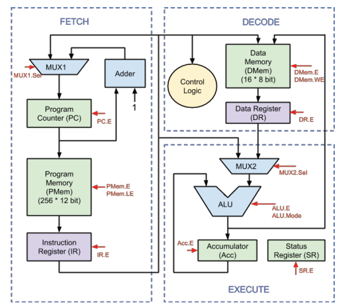
The following two type of components holds programming context.
- Program counter, program memory, data memory, accumulator, status register (green boxes). They are programmer visible registers and memories.
- Instruction register and data register (purple boxes). They are programmer invisible registers.
- ALU, MUX1, MUX2, Adder (blue boxes), used as a functional unit.
- Control Logic (yellow box), used to denote all control signals (red signal)
The timing and state transition are shown in the following diagram.
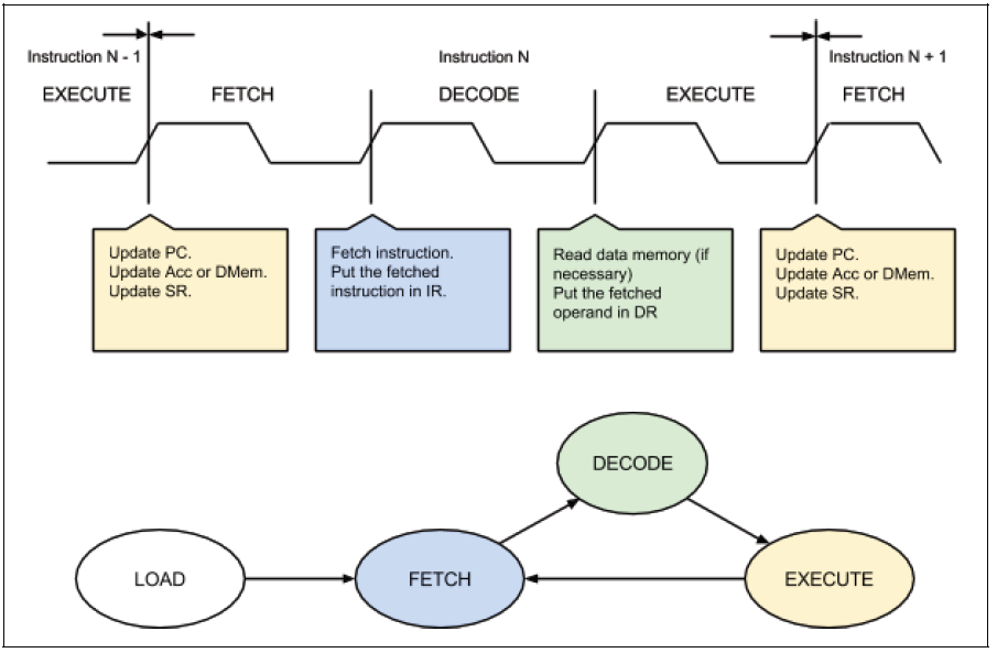
Each instruction needs 3 clock cycles to finish, i.e. FETCH stage, DECODE stage, and EXECUTE stage. Note that it is not pipelined. Together with the initial LOAD state, it can be considered as an FSM of 3 states (technically 4 states).
States:
1. LOAD (initial state): load program to program memory, which takes 1 cycle per instruction loaded;
2. FETCH (first cycle): fetch current instruction from program memory;
3. DECODE (second cycle): decode instruction to generate control logic, read data memory for operand;
4. EXECUTE (of the third cycle): execute instruction
Transitions:
- LOAD → FETCH (initialization finish):
- Clear content of PC, IR, DR, Acc, SR; DMem is not required to be cleared.
- FETCH → DECODE (rising edge of second cycle) :
- IR = PMem [ PC ]
- DECODE → EXECUTE
- DR = DMem [ IR[3:0] ];
- EXECUTE → FETCH (rising edge of first cycle and fourth cycle)
- For non-branch instruction, PC = PC + 1; for branch instruction, if branch is taken, PC = IR [7:0], otherwise PC = PC + 1;
- For ALU instruction, if the result destination is accumulator, Acc = ALU.Out; if the result destination is data memory, DMem [ IR[3:0] ] = ALU.Out.
- For ALU instruction, SR = ALU.Status;
The transitions can be simplified using enable port of corresponding registers, e.g. assign ALU.Out to Acc at every clock rising edge if Acc.E is set to 1. Such control signals as Acc.E are generated as a boolean function of both current state and the current instruction.
Components
Registers
The microcontroller has 3 programmer visible register:
- Program Counter (8 bit, denoted as PC): contains the index of current executing instruction.
- Accumulator (8 bit, denoted as Acc): holds result and 1 operand of the arithmetic or logic calculation.
- Status Register (4 bit, denoted as SR): holds 4 status bit, i.e. Z, C, S, O.
- Z (zero flag, SR[3]): 1 if result is zero, 0 otherwise.
- C (carry flag, SR[2]): 1 if carry is generated, 0 otherwise.
- S (sign flag, SR[1]): 1 if result is negative (as 2’s complement), 0 otherwise.
- O (overflow flag, SR[0]): 1 if result generates overflow, 0 otherwise.
Each of these registers has an enable port, as a flag for whether the value of the register should be updated in state transition. They are denoted as PC.E, Acc.E, and SR.E.
The microcontroller has 2 programmer invisible registers (i.e. they can not be manipulated by programmer):
- Instruction Register (12 bit, denoted as IR): contains the current executing instruction.
- Data Register (8 bit, denoted as DR): contains the operand read from data memory.
Similarly, each of these registers has an enable port as a flag for whether the value of the register should be updated in state transition. They are denoted as IR.E and DR.E.
Program memory
The microcontroller has a 256 entry program memory that stores program instructions, denoted as PMem. Each entry is 12 bits, the ith entry is denoted as PMem[i]. The program memory has the following input/output ports.
- Enable port (1 bit, input, denoted as PMem.E): enable the device, i.e. if it is 1, then the entry specified by the address port will be read out, otherwise, nothing is read out.
- Address port (8 bit, input, denoted as PMem.Addr): specify which instruction entry is read out, connected to PC.
- Instruction port (12 bit, output, denoted as PMem.I): the instruction entry that is read out, connected to IR.
- 3 special ports are used to load program to the memory, not used for executing instructions.
- Load enable port (1 bit, input, denoted as PMem.LE): enable the load, i.e. if it is 1, then the entry specified by the address port will be load with the value specified by the load instruction input port and the instruction port is supplied with the same value; otherwise, the entry specified by the address port will be read out on instruction port, and value on instruction load port is ignored.
- Load address port (8 bit, input, denoted as PMem.LA): specify which instruction entry is loaded.
- Load instruction port (12 bit, input, denoted as PMem.LI): the instruction that is loaded.
For example, if the address point is supplied with 8’b0000_0011 and enable is set to 1, the fourth entry is read out on instruction port.
Note that program load only takes effect on clock rising edge, while instruction read out happens all the time.
Data memory
The microcontroller has a 16 entry data memory, denoted as DMem. Each entry is 8 bits, the ith entry is denoted as DMem[i]. The program memory has the following input/output ports.
- Enable port (1 bit, input, denoted as DMem.E): enable the device, i.e. if it is 1, then the entry specified by the address port will be read out or written in; otherwise nothing is read out or written in.
- Write enable port(1 bit, input, denoted as DMem.WE): enable the write, i.e. if it is 1, then the entry specified by the address port will be written with the value specified by the data input port and the data output port is supplied with the same value; otherwise, the entry specified by the address port will be read out on data output port, and value on data input port is ignored.
- Address port (4 bit, input, denoted as DMem.Addr): specify which data entry is read out, connected to IR[3:0].
- Data input port (8 bit, input, denoted as DMem.DI): the value that is written in, connected to ALU.Out.
- Data output port (8 bit, output, denoted as DMem.DO): the data entry that is read out, connected to MUX2.In1.
For example, if the address point is supplied with 8’0000_0011, data input port is supplied with 8’0000_0000, enable is set to 1, and write enable is set to 1, the fourth entry of the data memory is written with value 0 and the data output port shows 8’0000_0000.
As another example, if the address point is supplied with 8’0000_0011, data input port is supplied with 8’0000_0000, enable is set to 1, while write enable is set to 0, the fourth entry of the data memory is read out on data output port.
Note that write only takes effect on clock rising edge, while read happens all the time, similar to program memory.
PC adder
PC adder is used to add PC by 1, i.e. move to the next instruction. This component is pure combinational. It has the following port.
- Adder input port (8 bit, input, denoted as Adder.In): connected to PC.
- Adder output port (8 bit, output, denoted as Adder.Out): connected to MUX1.In2.
MUX1
MUX1 is used to choose the source for updating PC. If the current instruction is not a branch or it is a branch but the branch is not taken, PC is incremented by 1; otherwise PC is set to the jumping target, i.e. IR [7:0]. It has the following port.
- MUX1 input 1 port (8 bit, input, denoted as MUX1.In1): connected to IR [7:0].
- MUX1 input 2 port (8 bit, input, denoted as MUX1.In2): connected to Adder.Out.
- MUX1 selection port (1 bit, input, denoted as MUX1.Sel): connected to control logic.
- MUX1 output port (8 bit, output, denoted as MUX1.Out): connected to PC.
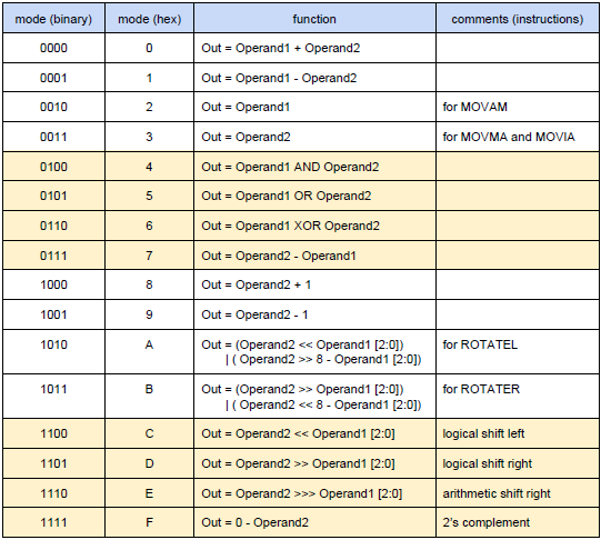
ALU
ALU is used to do the actual computation for the current instruction. This component is pure combinational. It has the following port. The mode of ALU is listed in the following table.
- ALU operand 1 port (8 bit, input, denoted as ALU.Operand1): connected to Acc.
- ALU operand 2 port (8 bit, input, denoted as ALU.Operand2): connected to MUX2.Out.
- ALU enable port (1 bit, input, denoted as ALU.E): connected to control logic.
- ALU mode port (4 bit, input, denoted as ALU.Mode): connected to control logic.
- Current flags port (4 bit, input, denoted as ALU.CFlags): connected to SR.
- ALU output port (8 bit, output, denoted as ALU.Out): connected to DMem.DI.
- ALU flags port (4 bit, output, denoted as ALU.Flags): the Z (zero), C (carry), S (sign), O (overflow) bits, from MSB to LSB, connected to status register.
MUX2
MUX2 is used to choose the source for operand 2 of ALU. If the current instruction is M type, operand 2 of ALU comes from data memory; if the current instruction is I type, operand 2 of ALU comes from the instruction, i.e. IR [7:0]. It has the following port.
- MUX2 input 1 port (8 bit, input, denoted as MUX2.In1): connected to IR [7:0].
- MUX2 input 2 port (8 bit, input, denoted as MUX2.In2): connected to DR.
- MUX2 selection port (1 bit, input, denoted as MUX2.Sel): connected to control logic.
- MUX2 output port (8 bit, output, denoted as MUX2.Out): connected to ALU.Operand2.
Control unit design
Control signal is derived from the current state and current instruction. The control logic component is purely combinational. There are in total 12 control signals, listed as follows.
- PC.E: enable port of program counter (PC);
- Acc.E: enable port of accumulator (Acc);
- SR.E: enable port of status register (SR);
- IR.E: enable port of instruction register (IR);
- DR.E: enable port of data register (DR);
- PMem.E: enable port of program memory (PMem);
- DMem.E: enable port of data memory (DMem);
- DMem.WE: write enable port of data memory (DMem);
- ALU.E: enable port of ALU;
- ALU.Mode: mode selection port of ALU;
- MUX1.Sel: selection port of MUX1;
- MUX2.Sel: selection port of MUX2;
The following table documents the detail of how these control signals are generated important signals are marked in red.
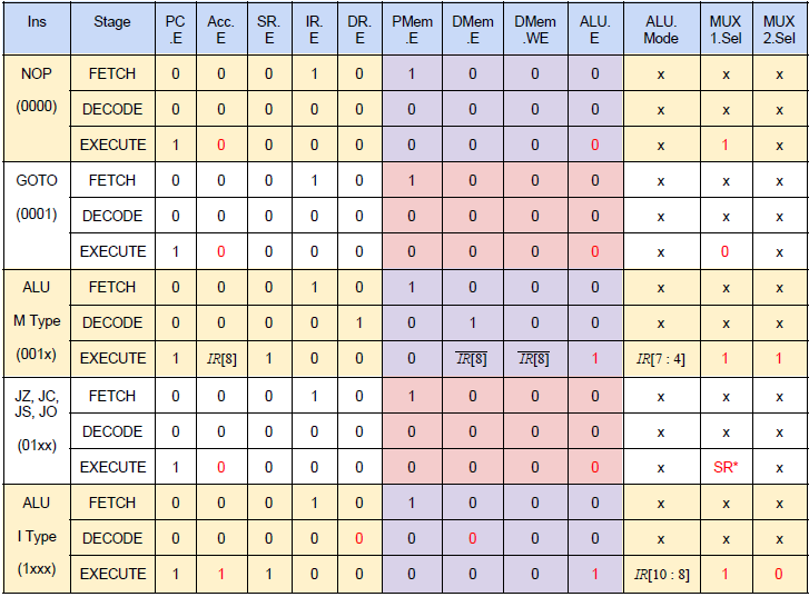
Comments:
1. Note that in EXECUTE state of conditional branch instructions, the value of MUX1.Sel is actually SR[ IR [9:8] ];
2. Note that in EXECUTE stage of ALU I type instruction, the value of ALU.Mode is actually {0, IR[10:8]}. In the table above, 0 extension is assumed.
3. Be careful that PMem.LE is not shown in this table. If the processor is not in LOAD state, PMem.LE is always set to 0.
The type and category of instruction can be identified by the first 4 bits of the instruction, i.e. IR[11:8], as denoted in the first column of the above table.
Besides, when loading the program, the control signal is generated as below.
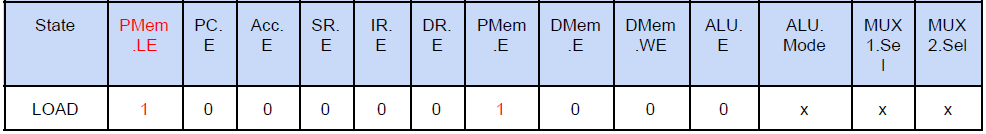
If the processor is in LOAD state, PMem.LE is always set to 1.
The Instruction Set Architecture of the microcontroller(Part-1)
Part 3 will be the Verilog code for the whole microcontroller.
You may like this:
32-bit 5-stage Pipelined MIPS Processor in Verilog (Part-1)
32-bit 5-stage Pipelined MIPS Processor in Verilog (Part-2)
32-bit 5-stage Pipelined MIPS Processor in Verilog (Part-3)
32-bit 5-stage Pipelined MIPS Processor in Verilog (Part-2)
32-bit 5-stage Pipelined MIPS Processor in Verilog (Part-3)
What is FPGA Programming? FPGA vs Software programming
Recommended and affordable Xilinx FPGA boards for students
Recommended and affordable Altera FPGA boards for students
Recommended and affordable Xilinx FPGA boards for students
Recommended and affordable Altera FPGA boards for students
Recommended Verilog projects:
2. Verilog code for FIFO memory
3. Verilog code for 16-bit single-cycle MIPS processor
4. Programmable Digital Delay Timer in Verilog HDL
5. Verilog code for basic logic components in digital circuits
6. Verilog code for 32-bit Unsigned Divider
7. Verilog code for Fixed-Point Matrix Multiplication
8. Plate License Recognition in Verilog HDL
9. Verilog code for Carry-Look-Ahead Multiplier
10. Verilog code for a Microcontroller
11. Verilog code for 4x4 Multiplier
12. Verilog code for Car Parking System
13. Image processing on FPGA using Verilog HDL
14. How to load a text file into FPGA using Verilog HDL
15. Verilog code for Traffic Light Controller
16. Verilog code for Alarm Clock on FPGA
17. Verilog code for comparator design
18. Verilog code for D Flip Flop
19. Verilog code for Full Adder
20. Verilog code for counter with testbench
21. Verilog code for 16-bit RISC Processor
22. Verilog code for button debouncing on FPGA
23. How to write Verilog Testbench for bidirectional/ inout ports
24. Tic Tac Toe Game in Verilog and LogiSim
25. 32-bit 5-stage Pipelined MIPS Processor in Verilog (Part-1)
26. 32-bit 5-stage Pipelined MIPS Processor in Verilog (Part-2)
27. 32-bit 5-stage Pipelined MIPS Processor in Verilog (Part-3)
28. Verilog code for Decoder25. 32-bit 5-stage Pipelined MIPS Processor in Verilog (Part-1)
26. 32-bit 5-stage Pipelined MIPS Processor in Verilog (Part-2)
27. 32-bit 5-stage Pipelined MIPS Processor in Verilog (Part-3)
29. Verilog code for Multiplexers
30. N-bit Adder Design in Verilog
31. Verilog vs VHDL: Explain by Examples
32. Verilog code for Clock divider on FPGA
33. How to generate a clock enable signal in Verilog
34. Verilog code for PWM Generator
35. Verilog coding vs Software Programming
36. Verilog code for Sequence Detector using Moore FSM
31. Verilog vs VHDL: Explain by Examples
32. Verilog code for Clock divider on FPGA
33. How to generate a clock enable signal in Verilog
34. Verilog code for PWM Generator
35. Verilog coding vs Software Programming
36. Verilog code for Sequence Detector using Moore FSM


Nice post. keep posting. thanks.
ReplyDeletePlease visit the next part:
Deletehttps://fpga4student.blogspot.com/2016/11/verilog-code-for-microcontroller.html
ERROR:Xst:2355 - "06. microcontroller_main.v" line 24: Value 167479828 found at line 1 is not binary in call of system task $readmemb.
ReplyDeleteGetting this error. Please help me.
"program_mem.dat". Did you create this file in the project folder? Create this file and copy the provided test program into this file and run simulation.
ReplyDelete