

In this project, a 16-bit single-cycle MIPS processor is implemented in Verilog HDL. MIPS is an RISC processor, which is widely used by many universities in academic courses related to computer organization and architecture.
The Instruction Format and Instruction Set Architecture for the 16-bit single-cycle MIPS are as follows:
 |
| Instruction set for the MIPS processor |
 |
| Instruction Set Architecture for the MIPS processor |
Below is the description for instructions being implemented in Verilog:
- Add : R[rd] = R[rs] + R[rt]
- Subtract : R[rd] = R[rs] - R[rt]
- And: R[rd] = R[rs] & R[rt]
- Or : R[rd] = R[rs] | R[rt]
- SLT: R[rd] = 1 if R[rs] < R[rt] else 0
- Jr: PC=R[rs]
- Lw: R[rt] = M[R[rs]+SignExtImm]
- Sw : M[R[rs]+SignExtImm] = R[rt]
- Beq : if(R[rs]==R[rt]) PC=PC+1+BranchAddr
- Addi: R[rt] = R[rs] + SignExtImm
- J : PC=JumpAddr
- Jal : R[7]=PC+2;PC=JumpAddr
- SLTI: R[rt] = 1 if R[rs] < imm else 0
SignExtImm = { 9{immediate[6]}, imm
JumpAddr = { (PC+1)[15:13], address}
BranchAddr = { 7{immediate[6]}, immediate, 1’b0 }
Based on the provided instruction set, the data-path and control unit are designed and implemented.
Control unit design:
Control signals
| |||||||||
Instruction
|
Reg
Dst
|
ALUSrc
|
Memto
Reg
|
Reg
Write
|
MemRead
|
Mem
Write
|
Branch
|
ALUOp
|
Jump
|
R-type
|
1
|
0
|
0
|
1
|
0
|
0
|
0
|
00
|
0
|
LW
|
0
|
1
|
1
|
1
|
1
|
0
|
0
|
11
|
0
|
SW
|
0
|
1
|
0
|
0
|
0
|
1
|
0
|
11
|
0
|
addi
|
0
|
1
|
0
|
1
|
0
|
0
|
0
|
11
|
0
|
beq
|
0
|
0
|
0
|
0
|
0
|
0
|
1
|
01
|
0
|
j
|
0
|
0
|
0
|
0
|
0
|
0
|
0
|
00
|
1
|
jal
|
2
|
0
|
2
|
1
|
0
|
0
|
0
|
00
|
1
|
slti
|
0
|
1
|
0
|
1
|
0
|
0
|
0
|
10
|
0
|
ALU Control
| ||||
ALU op
|
Function
|
ALUcnt
|
ALU Operation
|
Instruction
|
11
|
xxxx
|
000
|
ADD
|
Addi,lw,sw
|
01
|
xxxx
|
001
|
SUB
|
BEQ
|
00
|
00
|
000
|
ADD
|
R-type: ADD
|
00
|
01
|
001
|
SUB
|
R-type: sub
|
00
|
02
|
010
|
AND
|
R-type: AND
|
00
|
03
|
011
|
OR
|
R-type: OR
|
00
|
04
|
100
|
slt
|
R-type: slt
|
10
|
xxxxxx
|
100
|
slt
|
i-type: slti
|
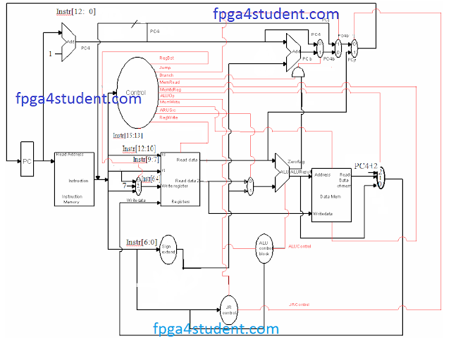 |
| Data-path and control unit of the 16-bit MIPS processor |
After completing the design for the MIPS processor, it is easy to write Verilog code for the MIPS processor. The Verilog code for the whole design of the MIPS processor as follows:
Verilog code for ALU unit
Verilog code for register file
Verilog code for instruction memory
It is quite simple to verify the Verilog code for the single-cycle MIPS CPU by doing several simulations on ModelSim or Xilinx ISIM in order to see how the MIPS processor works. To fully verify the MIPS processor, it is needed to modify the instruction memory to simulate all the instructions in the instruction set architecture, and then check simulation waveform and memory to see if the processor works correctly as designed.
You may like this:
32-bit 5-stage Pipelined MIPS Processor in Verilog (Part-1)
32-bit 5-stage Pipelined MIPS Processor in Verilog (Part-2)
32-bit 5-stage Pipelined MIPS Processor in Verilog (Part-3)
Verilog code for 16-bit RISC Processor
VHDL code for MIPS Processor
29. Verilog code for Multiplexers
Verilog code for register file
Verilog code for instruction memory
Verilog code for data memory:
//fpga4student.com: FPGA projects, Verilog projects, VHDL projects
// Verilog project: Verilog code for 16-bit MIPS Processor
// Submodule: Data memory in Verilog
 module data_memory
 (
      input                         clk,
      // address input, shared by read and write port
      input     [15:0]               mem_access_addr,
      // write port
      input     [15:0]               mem_write_data,
      input                         mem_write_en,
      input mem_read,
      // read port
      output     [15:0]               mem_read_data
 );
      integer i;
      reg [15:0] ram [255:0];
      wire [7 : 0] ram_addr = mem_access_addr[8 : 1];
      initial begin
           for(i=0;i<256;i=i+1)
                ram[i] <= 16'd0;
      end
      always @(posedge clk) begin
           if (mem_write_en)
                ram[ram_addr] <= mem_write_data;
      end
      assign mem_read_data = (mem_read==1'b1) ? ram[ram_addr]: 16'd0;
 endmodule
Verilog code for ALU Control unit:
//fpga4student.com: FPGA projects, Verilog projects, VHDL projects
// Verilog project: Verilog code for 16-bit MIPS Processor
// Submodule: ALU Control Unit in Verilog
 module ALUControl( ALU_Control, ALUOp, Function);
 output reg[2:0] ALU_Control;
 input [1:0] ALUOp;
 input [3:0] Function;
 wire [5:0] ALUControlIn;
 assign ALUControlIn = {ALUOp,Function};
 always @(ALUControlIn)
 casex (ALUControlIn)
  6'b11xxxx: ALU_Control=3'b000;
  6'b10xxxx: ALU_Control=3'b100;
  6'b01xxxx: ALU_Control=3'b001;
  6'b000000: ALU_Control=3'b000;
  6'b000001: ALU_Control=3'b001;
  6'b000010: ALU_Control=3'b010;
  6'b000011: ALU_Control=3'b011;
  6'b000100: ALU_Control=3'b100;
  default: ALU_Control=3'b000;
  endcase
 endmodule
// Verilog code for JR control unit
module JR_Control( input[1:0] alu_op,
       input [3:0] funct,
       output JRControl
    );
assign JRControl = ({alu_op,funct}==6'b001000) ? 1'b1 : 1'b0;
endmodule
Verilog code for control unit:
//fpga4student.com: FPGA projects, Verilog projects, VHDL projects
// Verilog project: Verilog code for 16-bit MIPS Processor
// Submodule: Control Unit in Verilog
 module control( input[2:0] opcode,
                           input reset,
                           output reg[1:0] reg_dst,mem_to_reg,alu_op,
                           output reg jump,branch,mem_read,mem_write,alu_src,reg_write,sign_or_zero
   );
 always @(*)
 begin
      if(reset == 1'b1) begin
                reg_dst = 2'b00;
                mem_to_reg = 2'b00;
                alu_op = 2'b00;
                jump = 1'b0;
                branch = 1'b0;
                mem_read = 1'b0;
                mem_write = 1'b0;
                alu_src = 1'b0;
                reg_write = 1'b0;
                sign_or_zero = 1'b1;
      end
      else begin
      case(opcode)
      3'b000: begin // add
                reg_dst = 2'b01;
                mem_to_reg = 2'b00;
                alu_op = 2'b00;
                jump = 1'b0;
                branch = 1'b0;
                mem_read = 1'b0;
                mem_write = 1'b0;
                alu_src = 1'b0;
                reg_write = 1'b1;
                sign_or_zero = 1'b1;
                end
      3'b001: begin // sli
                reg_dst = 2'b00;
                mem_to_reg = 2'b00;
                alu_op = 2'b10;
                jump = 1'b0;
                branch = 1'b0;
                mem_read = 1'b0;
                mem_write = 1'b0;
                alu_src = 1'b1;
                reg_write = 1'b1;
                sign_or_zero = 1'b0;
                end
      3'b010: begin // j
                reg_dst = 2'b00;
                mem_to_reg = 2'b00;
                alu_op = 2'b00;
                jump = 1'b1;
                branch = 1'b0;
                mem_read = 1'b0;
                mem_write = 1'b0;
                alu_src = 1'b0;
                reg_write = 1'b0;
                sign_or_zero = 1'b1;
                end
      3'b011: begin // jal
                reg_dst = 2'b10;
                mem_to_reg = 2'b10;
                alu_op = 2'b00;
                jump = 1'b1;
                branch = 1'b0;
                mem_read = 1'b0;
                mem_write = 1'b0;
                alu_src = 1'b0;
                reg_write = 1'b1;
                sign_or_zero = 1'b1;
                end
      3'b100: begin // lw
                reg_dst = 2'b00;
                mem_to_reg = 2'b01;
                alu_op = 2'b11;
                jump = 1'b0;
                branch = 1'b0;
                mem_read = 1'b1;
                mem_write = 1'b0;
                alu_src = 1'b1;
                reg_write = 1'b1;
                sign_or_zero = 1'b1;
                end
      3'b101: begin // sw
                reg_dst = 2'b00;
                mem_to_reg = 2'b00;
                alu_op = 2'b11;
                jump = 1'b0;
                branch = 1'b0;
                mem_read = 1'b0;
                mem_write = 1'b1;
                alu_src = 1'b1;
                reg_write = 1'b0;
                sign_or_zero = 1'b1;
                end
      3'b110: begin // beq
                reg_dst = 2'b00;
                mem_to_reg = 2'b00;
                alu_op = 2'b01;
                jump = 1'b0;
                branch = 1'b1;
                mem_read = 1'b0;
                mem_write = 1'b0;
                alu_src = 1'b0;
                reg_write = 1'b0;
                sign_or_zero = 1'b1;
                end
      3'b111: begin // addi
                reg_dst = 2'b00;
                mem_to_reg = 2'b00;
                alu_op = 2'b11;
                jump = 1'b0;
                branch = 1'b0;
                mem_read = 1'b0;
                mem_write = 1'b0;
                alu_src = 1'b1;
                reg_write = 1'b1;
                sign_or_zero = 1'b1;
                end
      default: begin
                reg_dst = 2'b01;
                mem_to_reg = 2'b00;
                alu_op = 2'b00;
                jump = 1'b0;
                branch = 1'b0;
                mem_read = 1'b0;
                mem_write = 1'b0;
                alu_src = 1'b0;
                reg_write = 1'b1;
                sign_or_zero = 1'b1;
                end
      endcase
      end
 end
 endmodule
Verilog code for the single-cycle MIPS processor:
//fpga4student.com: FPGA projects, Verilog projects, VHDL projects
// Verilog project: Verilog code for 16-bit MIPS Processor
 // Verilog code for 16 bit single cycle MIPS CPU
 module mips_16( input clk,reset,
                           output[15:0] pc_out, alu_result
                           //,reg3,reg4
   );
 reg[15:0] pc_current;
 wire signed[15:0] pc_next,pc2;
 wire [15:0] instr;
 wire[1:0] reg_dst,mem_to_reg,alu_op;
 wire jump,branch,mem_read,mem_write,alu_src,reg_write     ;
 wire     [2:0]     reg_write_dest;
 wire     [15:0] reg_write_data;
 wire     [2:0]     reg_read_addr_1;
 wire     [15:0] reg_read_data_1;
 wire     [2:0]     reg_read_addr_2;
 wire     [15:0] reg_read_data_2;
 wire [15:0] sign_ext_im,read_data2,zero_ext_im,imm_ext;
 wire JRControl;
 wire [2:0] ALU_Control;
 wire [15:0] ALU_out;
 wire zero_flag;
 wire signed[15:0] im_shift_1, PC_j, PC_beq, PC_4beq,PC_4beqj,PC_jr;
 wire beq_control;
 wire [14:0] jump_shift_1;
 wire [15:0]mem_read_data;
 wire [15:0] no_sign_ext;
 wire sign_or_zero;
 // PC
 always @(posedge clk or posedge reset)
 begin
      if(reset)
           pc_current <= 16'd0;
      else
           pc_current <= pc_next;
 end
 // PC + 2
 assign pc2 = pc_current + 16'd2;
 // instruction memory
 instr_mem instrucion_memory(.pc(pc_current),.instruction(instr));
 // jump shift left 1
 assign jump_shift_1 = {instr[13:0],1'b0};
 // control unit
 control control_unit(.reset(reset),.opcode(instr[15:13]),.reg_dst(reg_dst)
                ,.mem_to_reg(mem_to_reg),.alu_op(alu_op),.jump(jump),.branch(branch),.mem_read(mem_read),
                .mem_write(mem_write),.alu_src(alu_src),.reg_write(reg_write),.sign_or_zero(sign_or_zero));
 // multiplexer regdest
 assign reg_write_dest = (reg_dst==2'b10) ? 3'b111: ((reg_dst==2'b01) ? instr[6:4] :instr[9:7]);
 // register file
 assign reg_read_addr_1 = instr[12:10];
 assign reg_read_addr_2 = instr[9:7];
 register_file reg_file(.clk(clk),.rst(reset),.reg_write_en(reg_write),
 .reg_write_dest(reg_write_dest),
 .reg_write_data(reg_write_data),
 .reg_read_addr_1(reg_read_addr_1),
 .reg_read_data_1(reg_read_data_1),
 .reg_read_addr_2(reg_read_addr_2),
 .reg_read_data_2(reg_read_data_2));
 //.reg3(reg3),
 //.reg4(reg4));
 // sign extend
 assign sign_ext_im = {{9{instr[6]}},instr[6:0]};
 assign zero_ext_im = {{9{1'b0}},instr[6:0]};
 assign imm_ext = (sign_or_zero==1'b1) ? sign_ext_im : zero_ext_im;
 // JR control
 JR_Control JRControl_unit(.alu_op(alu_op),.funct(instr[3:0]),.JRControl(JRControl));
 // ALU control unit
 ALUControl ALU_Control_unit(.ALUOp(alu_op),.Function(instr[3:0]),.ALU_Control(ALU_Control));
 // multiplexer alu_src
 assign read_data2 = (alu_src==1'b1) ? imm_ext : reg_read_data_2;
 // ALU
 alu alu_unit(.a(reg_read_data_1),.b(read_data2),.alu_control(ALU_Control),.result(ALU_out),.zero(zero_flag));
 // immediate shift 1
 assign im_shift_1 = {imm_ext[14:0],1'b0};
 //
 assign no_sign_ext = ~(im_shift_1) + 1'b1;
 // PC beq add
 assign PC_beq = (im_shift_1[15] == 1'b1) ? (pc2 - no_sign_ext): (pc2 +im_shift_1);
 // beq control
 assign beq_control = branch & zero_flag;
 // PC_beq
 assign PC_4beq = (beq_control==1'b1) ? PC_beq : pc2;
 // PC_j
 assign PC_j = {pc2[15],jump_shift_1};
 // PC_4beqj
 assign PC_4beqj = (jump == 1'b1) ? PC_j : PC_4beq;
 // PC_jr
 assign PC_jr = reg_read_data_1;
 // PC_next
 assign pc_next = (JRControl==1'b1) ? PC_jr : PC_4beqj;
 // data memory
 data_memory datamem(.clk(clk),.mem_access_addr(ALU_out),
 .mem_write_data(reg_read_data_2),.mem_write_en(mem_write),.mem_read(mem_read),
 .mem_read_data(mem_read_data));
 // write back
 assign reg_write_data = (mem_to_reg == 2'b10) ? pc2:((mem_to_reg == 2'b01)? mem_read_data: ALU_out);
 // output
 assign pc_out = pc_current;
 assign alu_result = ALU_out;
 endmodule
Verilog testbench code for the single-cycle MIPS processor:
 `timescale 1ns / 1ps
//fpga4student.com: FPGA projects, Verilog projects, VHDL projects
// Verilog project: Verilog code for 16-bit MIPS Processor
// Testbench Verilog code for 16 bit single cycle MIPS CPU
 module tb_mips16;
      // Inputs
      reg clk;
      reg reset;
      // Outputs
      wire [15:0] pc_out;
      wire [15:0] alu_result;//,reg3,reg4;
      // Instantiate the Unit Under Test (UUT)
      mips_16 uut (
           .clk(clk),
           .reset(reset),
           .pc_out(pc_out),
           .alu_result(alu_result)
           //.reg3(reg3),
          // .reg4(reg4)
      );
      initial begin
           clk = 0;
           forever #10 clk = ~clk;
      end
      initial begin
           // Initialize Inputs
           //$monitor ("register 3=%d, register 4=%d", reg3,reg4);
           reset = 1;
           // Wait 100 ns for global reset to finish
           #100;
     reset = 0;
           // Add stimulus here
      end
 endmodule
Source code provided by
Abdrazak Mohammed Anana
Abdrazak Mohammed Anana
32-bit 5-stage Pipelined MIPS Processor in Verilog (Part-1)
32-bit 5-stage Pipelined MIPS Processor in Verilog (Part-2)
32-bit 5-stage Pipelined MIPS Processor in Verilog (Part-3)
Verilog code for 16-bit RISC Processor
VHDL code for MIPS Processor
Recommended Verilog projects:
2. Verilog code for FIFO memory
3. Verilog code for 16-bit single-cycle MIPS processor
4. Programmable Digital Delay Timer in Verilog HDL
5. Verilog code for basic logic components in digital circuits
6. Verilog code for 32-bit Unsigned Divider
7. Verilog code for Fixed-Point Matrix Multiplication
8. Plate License Recognition in Verilog HDL
9. Verilog code for Carry-Look-Ahead Multiplier
10. Verilog code for a Microcontroller
11. Verilog code for 4x4 Multiplier
12. Verilog code for Car Parking System
13. Image processing on FPGA using Verilog HDL
14. How to load a text file into FPGA using Verilog HDL
15. Verilog code for Traffic Light Controller
16. Verilog code for Alarm Clock on FPGA
17. Verilog code for comparator design
18. Verilog code for D Flip Flop
19. Verilog code for Full Adder
20. Verilog code for counter with testbench
21. Verilog code for 16-bit RISC Processor
22. Verilog code for button debouncing on FPGA
23. How to write Verilog Testbench for bidirectional/ inout ports
24. Tic Tac Toe Game in Verilog and LogiSim
25. 32-bit 5-stage Pipelined MIPS Processor in Verilog (Part-1)
26. 32-bit 5-stage Pipelined MIPS Processor in Verilog (Part-2)
27. 32-bit 5-stage Pipelined MIPS Processor in Verilog (Part-3)
28. Verilog code for Decoder25. 32-bit 5-stage Pipelined MIPS Processor in Verilog (Part-1)
26. 32-bit 5-stage Pipelined MIPS Processor in Verilog (Part-2)
27. 32-bit 5-stage Pipelined MIPS Processor in Verilog (Part-3)
29. Verilog code for Multiplexers
31. Verilog vs VHDL: Explain by Examples
32. Verilog code for Clock divider on FPGA
33. How to generate a clock enable signal in Verilog
34. Verilog code for PWM Generator
35. Verilog coding vs Software Programming
36. Verilog code for Moore FSM Sequence Detector
37. Verilog code for 7-segment display controller on Basys 3 FPGA
32. Verilog code for Clock divider on FPGA
33. How to generate a clock enable signal in Verilog
34. Verilog code for PWM Generator
35. Verilog coding vs Software Programming
36. Verilog code for Moore FSM Sequence Detector
37. Verilog code for 7-segment display controller on Basys 3 FPGA


May i check with you what type of stimulus do i have to include in the test bench codes. I ran the whole program with the testbench for 100ns but the register values are 0 or x
ReplyDeleteHow did you apply stimulus
DeleteDouble check your instruction memory. All instructions here are fully verified.
ReplyDeleteYou can check instruction by instruction and see register files, data memory to verify.
Ok thanks for your advice. And i have another problem, when i compile the program, i have this error:
ReplyDeleteError (12006): Node instance "JR_Control_unit" instantiates undefined entity "JR_Control"
Anybody knows how to solve it?
module JR_Control( input[1:0] alu_op,
ReplyDeleteinput [3:0] funct,
output JRControl
);
assign JRControl = ({alu_op,funct}==6'b001000) ? 1'b1 : 1'b0;
endmodule
Here it is
Thank you so much for your help!
DeleteWhat is
Deleteport ' ' reg 3 ' ' is not a port of reg_file
port ' ' reg 4 ' ' is not a port of reg_file
in mips_16_bit module
How do i implement a pipeline structure into a mips processor? Do i just implement a register in between individual stages? If so where do i implement them.
ReplyDeleteThere will be a pipe-lined MIPS in Verilog post soon.
ReplyDeletecan anybdy please explain the working, i shall be very greatful..plz
ReplyDeleteI am getting the errors:
ReplyDeleteport ' ' reg 3 ' ' is not a port of reg_file
port ' ' reg 4 ' ' is not a port of reg_file
Any help? :-)
`timescale 1ns / 1ps
ReplyDeletemodule register_file
( //fpga4student.com: FPga projects, Verilog projects, VHDL projects
input clk,
input rst,
// write port
input reg_write_en,
input [2:0] reg_write_dest,
input [15:0] reg_write_data,
//read port 1
input [2:0] reg_read_addr_1,
output [15:0] reg_read_data_1,
//read port 2
input [2:0] reg_read_addr_2,
output [15:0] reg_read_data_2
);
reg [15:0] reg_array [7:0];
// write port
//reg [2:0] i;
always @ (posedge clk or posedge rst) begin
if(rst) begin
reg_array[0] <= 15'b0;
reg_array[1] <= 15'b0;
reg_array[2] <= 15'b0;
reg_array[3] <= 15'b0;
reg_array[4] <= 15'b0;
reg_array[5] <= 15'b0;
reg_array[6] <= 15'b0;
reg_array[7] <= 15'b0;
end
else begin
if(reg_write_en) begin
reg_array[reg_write_dest] <= reg_write_data;
end
end
end
assign reg_read_data_1 = ( reg_read_addr_1 == 0)? 15'b0 : reg_array[reg_read_addr_1];
assign reg_read_data_2 = ( reg_read_addr_2 == 0)? 15'b0 : reg_array[reg_read_addr_2];
endmodule
I tried that but the end output just outputs 'z's??? I guess I dont know what is supposed to be happening here
DeletePlease post verilog codes for 32 bit pipelined risc processor with data path and control unit explanation
ReplyDeletehttp://www.fpga4student.com/2017/06/32-bit-pipelined-mips-processor-in-verilog-1.html
Deletehttp://www.fpga4student.com/2017/06/32-bit-pipelined-mips-processor-in-verilog-2.html
http://www.fpga4student.com/2017/06/32-bit-pipelined-mips-processor-in-verilog-3.html
Kindly check it out the Verilog code for 32-bit pipelined processor
port ' ' reg 3 ' ' is not a port of reg_file
ReplyDeleteport ' ' reg 4 ' ' is not a port of reg_file
That's only for debugging in simulation.
DeleteYou can easily add reg3 = reg_array[3] or reg4 = reg_array[4].
You can commented it out in the top level code if you don't want to see it in simulation.
http://www.fpga4student.com/2017/06/32-bit-pipelined-mips-processor-in-verilog-1.html
ReplyDeletehttp://www.fpga4student.com/2017/06/32-bit-pipelined-mips-processor-in-verilog-2.html
http://www.fpga4student.com/2017/06/32-bit-pipelined-mips-processor-in-verilog-3.html
Kindly check it out the Verilog code for 32-bit pipelined processor
sir where is JR_Control code for the 16 bits MIPS ?
ReplyDeleteUpdated in the ALU Control unit. Thanks.
Deletewhat is difference between 16 bit risk and 16 bit mips processor.I read that mips is risk based processor!
ReplyDeleteI already mentioned in the post, MIPS is a RISC processor.
DeleteI have a question at "wire [7 : 0] ram_addr = mem_access_addr[9 : 2];" in the data memory.
ReplyDeleteIsn't it a 16 bits per word memory? I think it can be written with "wire [7 : 0] ram_addr = mem_access_addr[7 : 0];. Just a memory word alignments a MIPS data access unit.
Thanks for your question. It is a 16-bit CPU, so 2 byte per word. The PC and the Offset address is increased by 2. So ram_addr = mem_access_addr[8:1] or rom_addr=PC[4:1].
DeleteIf you use wire [7 : 0] ram_addr = mem_access_addr[7 : 0], the odd address(1,3,5,7, etc) will be omitted.
Verilog code for Programmable Priority Encoder?
ReplyDeleteThanks for your suggestion.
Deletei moved all files on quartus , but how do i test it?
ReplyDeletecan someone please post the 3 STAGE verilog code for single cycle MIPS processor (32 BITS)
ReplyDeleteCan i able to implement this is code is iverilog?
ReplyDeletesince if we use loop the compiler will show error as incomprehensible loop..
Please provide the code for Design a single-cycle MIPS-based (32-bit) processor using Verilog for the instructions such as R-type (ADD, SUB, AND, OR, SLT), I/M-type (LW/SW/ADDI/SUBI) and BEQ and J-type
ReplyDeleteinstructions (JAL, J). Consider only integer type of operation.
How to add stimulus??
ReplyDeleteHi,
ReplyDeleteAt RTL level, this code is correctly giving the results but on synthesizing this code, it is giving an error. Any idea how to resolve this?
Has anyone able to do post synthesis simulation on this.
Thanks.
what about alu_unit and instruction_memory kindly share code please
ReplyDeleteall the codes are shared, the links for these two are shared in the post too.
Delete