

This project is to present the Verilog code for a 32-bit pipelined MIPS Processor. In part 2, I presented all the Verilog code for the single-cycle MIPS datapath.
In this part, pipelined registers are added to complete the pipelined MIPS Processor. Verilog code for the complete 32-bit pipelined MIPS processor will be presented.
Below is the complete data path for the 32-bit 5-stage pipelined MIPS Processor after adding Pipelined Registers, Forwarding Unit, Stall Control Unit, and Flush Control Unit to the single-cycle datapath. Forwarding, Stall Control, and Flush Control units are designed to solve data and control hazards in the pipelined MIPS processor. Following are the detailed explanation for the hazard-solving modules and the complete pipelined MIPS processor in Verilog.
 |
| Pipelined MIPS Processor Datapath |
Forwarding Unit:
The Forwarding Unit is designed to solve the data hazards in pipelined MIPS Processor. The correct data at the output of the ALU is forwarded to the input of the ALU when data hazards are detected. Data hazards are detected when the source register (EX_rs or EX_rt) of the current instruction is the same as the destination register (MEM_WriteRegister or EX_WriteRegister) of the previous instruction.

Verilog code for Forwarding Unit:
`timescale 1 ps / 100 fs
// fpga4student.com: FPGA projects, Verilog Projects, VHDL projects
// Verilog project: 32-bit 5-stage Pipelined MIPS Processor in Verilog
// Forwarding Unit
module ForwardingUnit(ForwardA,ForwardB,MEM_RegWrite,WB_RegWrite,MEM_WriteRegister,WB_WriteRegister,EX_rs,EX_rt);
output [1:0] ForwardA,ForwardB;
wire [1:0] ForwardA,ForwardB;
input MEM_RegWrite,WB_RegWrite;
input [4:0] MEM_WriteRegister,WB_WriteRegister,EX_rs,EX_rt;

// a= 1 if ( MEM_WriteRegister != 0 )
or #(50) orMEM_WriteReg(a,MEM_WriteRegister[4],MEM_WriteRegister[3],MEM_WriteRegister[2],MEM_WriteRegister[1],MEM_WriteRegister[0]);
CompareAddress CompMEM_WriteReg_EXrs(b,MEM_WriteRegister,EX_rs);
and #(50) andx(x,MEM_RegWrite,a,b);
// x=1 if ((MEM_RegWrite==1)&&(MEM_WriteRegister != 0)&&(MEM_WriteRegister==EX_rs))

// c= 1 if ( WB_WriteRegister != 0 )
or #(50) orWB_WriteReg(c,WB_WriteRegister[4],WB_WriteRegister[3],WB_WriteRegister[2],WB_WriteRegister[1],WB_WriteRegister[0]);
CompareAddress CompWB_WriteReg_EXrs(d,WB_WriteRegister,EX_rs);
and #(50) andy(y,WB_RegWrite,c,d);
// y=1 if ((WB_RegWrite==1)&&(WB_WriteRegister != 0)&&(WB_WriteRegister==EX_rs))

// ForwardA[1] = x; va ForwardA[0] = (NOT x). y ;
assign ForwardA[1] = x;
not #(50) notxgate(notx,x);
and #(50) NOTxANDy(ForwardA[0],notx,y);

// ForwardB
CompareAddress CompMEM_WriteReg_EXrt(b1,MEM_WriteRegister,EX_rt);
CompareAddress CompWB_WriteReg_EXrt(d1,WB_WriteRegister,EX_rt);
and #(50) andx1(x1,MEM_RegWrite,a,b1);
and #(50) andy1(y1,WB_RegWrite,c,d1);

assign ForwardB[1] = x1;
not #(50) notx1gate(notx1,x1);
and #(50) NOTx1ANDy1(ForwardB[0],notx1,y1);
endmodule
After adding the forwarding unit to solve the data hazard, the 2x32 to 32 multiplexers at the input of the ALU become 3x32 to 32 multiplexers.
Verilog code for the multiplexer:
`timescale 1 ps / 100 fs
// fpga4student.com: FPGA projects, Verilog Projects, VHDL projects
// Verilog project: 32-bit 5-stage Pipelined MIPS Processor in Verilog
// mux3x32to32
module mux3x32to32(DataOut,A,B,C,Select);
output [31:0] DataOut;
input [1:0] Select;
input [31:0] A,B,C;
wire [31:0] DataOut1,DataOut2;

mux2x32to32 muxAB(DataOut1,A,B, Select[1]);
mux2x32to32 muxCA(DataOut2,C,A, Select[1]);
mux2x32to32 muxABC(DataOut,DataOut1,DataOut2, Select[0]);

endmodule
Next, Stall Control Unit is needed when data hazards occur and it needs to delay 1 cycle before forwarding.
Stall Control Unit:
Data hazards which needs stalling 1 cycle happen when the destination register (EX_rt) of the current reading memory instruction is the same as the source register (ID_rs or ID_rt) of the coming instruction in ID stage except for ID_rt of XORI and LW instructions (where Rt is the destination register not source register with XORI and LW).


Verilog code for Stall Control Unit:
`timescale 1 ps / 100 fs
// fpga4student.com: FPGA projects, Verilog Projects, VHDL projects
// Verilog project: 32-bit 5-stage Pipelined MIPS Processor in Verilog
// Stall Control
module StallControl(PC_WriteEn,IFID_WriteEn,Stall_flush,EX_MemRead,EX_rt,ID_rs,ID_rt,ID_Op);
output PC_WriteEn,IFID_WriteEn,Stall_flush;
wire PC_WriteEn,IFID_WriteEn,Stall_flush;
input EX_MemRead,EX_rt,ID_rs,ID_rt;
input [5:0] ID_Op;
wire [4:0] EX_rt,ID_rs,ID_rt,xorRsRt,xorRtRt;
wire [5:0] xoropcodelw,xoropcodexori;
wire EX_MemRead;
//wire xoropcode1,xoroprt;
// write in behavior model
/*always @(EX_MemRead or EX_rt or ID_rs or ID_rt)
begin
 if ((EX_MemRead==1)&&((EX_rt==ID_rs)||((EX_rt==ID_rt)&&(Opcode!= 6'b001110)&&(Opcode!= 6'b100011)))
  begin
  PC_WriteEn=1'b0;
  IFID_WriteEn=1'b0;
  Stall_flush =1'b1;
  end
  else
  begin
  PC_WriteEn=1'b1;
  IFID_WriteEn=1'b1;
  Stall_flush =1'b0;
  end
end
*/
// write in structural model
xor #(50) xorRsRt4(xorRsRt[4],EX_rt[4],ID_rs[4]);
xor #(50) xorRsRt3(xorRsRt[3],EX_rt[3],ID_rs[3]);
xor #(50) xorRsRt2(xorRsRt[2],EX_rt[2],ID_rs[2]);
xor #(50) xorRsRt1(xorRsRt[1],EX_rt[1],ID_rs[1]);
xor #(50) xorRsRt0(xorRsRt[0],EX_rt[0],ID_rs[0]);
or #(50) OrRsRt1(OrRsRt,xorRsRt[4],xorRsRt[3],xorRsRt[2],xorRsRt[1],xorRsRt[0]);
not #(50) notgate1(notOrRsRt,OrRsRt);
// neu EX_rt==ID_rs thi notOrRsRt = 1

xor #(50) xorRtRt4(xorRtRt[4],EX_rt[4],ID_rt[4]);
xor #(50) xorRtRt3(xorRtRt[3],EX_rt[3],ID_rt[3]);
xor #(50) xorRtRt2(xorRtRt[2],EX_rt[2],ID_rt[2]);
xor #(50) xorRtRt1(xorRtRt[1],EX_rt[1],ID_rt[1]);
xor #(50) xorRtRt0(xorRtRt[0],EX_rt[0],ID_rt[0]);
or #(50) OrRtRt1(OrRtRt,xorRtRt[4],xorRtRt[3],xorRtRt[2],xorRtRt[1],xorRtRt[0]);
not #(50) notgate2(notOrRtRt,OrRtRt);
// neu EX_rt==ID_rt thi notOrRtRt = 1
xor #(50) xoropcode5(xoropcodelw[5],ID_Op[5],1'b1);
xor #(50) xoropcode4(xoropcodelw[4],ID_Op[4],1'b0);
xor #(50) xoropcode3(xoropcodelw[3],ID_Op[3],1'b0);
xor #(50) xoropcode2(xoropcodelw[2],ID_Op[2],1'b0);
xor #(50) xoropcode1(xoropcodelw[1],ID_Op[1],1'b1);
xor #(50) xoropcode0(xoropcodelw[0],ID_Op[0],1'b1);
or #(50) oropcode1(ec1,xoropcodelw[5],xoropcodelw[4],xoropcodelw[3],xoropcodelw[2],xoropcodelw[1],xoropcodelw[0]);
// opcode != opcode[lw] xoropcodelw =1
xor #(50) xoropcod5(xoropcodexori[5],ID_Op[5],1'b0);
xor #(50) xoropcod4(xoropcodexori[4],ID_Op[4],1'b0);
xor #(50) xoropcod3(xoropcodexori[3],ID_Op[3],1'b1);
xor #(50) xoropcod2(xoropcodexori[2],ID_Op[2],1'b1);
xor #(50) xoropcod1(xoropcodexori[1],ID_Op[1],1'b1);
xor #(50) xoropcod0(xoropcodexori[0],ID_Op[0],1'b0);
or #(50) oropcode2(ec2,xoropcodexori[5],xoropcodexori[4],xoropcodexori[3],xoropcodexori[2],xoropcodexori[1],xoropcodexori[0]);
// opcode != opcode[xori] xoropcodexori =1

and #(50) and1(xorop,ec1,ec2);
and #(50) and2(xoroprt,xorop,notOrRtRt);
or #(50) OrEXIDRsRt(OrOut,notOrRsRt,xoroprt);
and #(50) AndCondition(Condition,EX_MemRead,OrOut);
// Condition =1 when stall is satisfied
not #(50) NotPC_WriteEn(PC_WriteEn,Condition);
not #(50) NotIFID_WriteEn(IFID_WriteEn,Condition);
buf #(50) bufStallflush(Stall_flush,Condition);
endmodule
Flush Control Unit:
Flush Control Unit is designed to solve control hazards and it discards instructions in IF and ID stages when a jump instruction(J, JR, or BNE) performs.
Verilog code for Flush Control units:
// fpga4student.com: FPGA projects, Verilog Projects, VHDL projects
// Verilog project: 32-bit 5-stage Pipelined MIPS Processor in Verilog
// Flush control signals
`timescale 1 ps / 100 fs
module flush_block(
ID_RegDst,ID_ALUSrc, ID_MemtoReg,ID_RegWrite,ID_MemRead,ID_MemWrite,
ID_Branch,ID_ALUOp,ID_JRControl,flush,RegDst,ALUSrc,MemtoReg,RegWrite,
MemRead,MemWrite,Branch,ALUOp,JRControl);

output ID_RegDst,ID_ALUSrc,ID_MemtoReg,ID_RegWrite,ID_MemRead,ID_MemWrite,ID_Branch,ID_JRControl;
output [1:0] ID_ALUOp;
input flush,RegDst,ALUSrc,MemtoReg,RegWrite,MemRead,MemWrite,Branch,JRControl;
input [1:0] ALUOp;

not #50 (notflush,flush);
and #50 and1(ID_RegDst,RegDst,notflush);
and #50 and2(ID_ALUSrc,ALUSrc,notflush);
and #50 and3(ID_MemtoReg,MemtoReg,notflush);
and #50 and4(ID_RegWrite,RegWrite,notflush);
and #50 and5(ID_MemRead,MemRead,notflush);
and #50 and6(ID_MemWrite,MemWrite,notflush);
and #50 and7(ID_Branch,Branch,notflush);
and #50 and8(ID_JRControl,JRControl,notflush);
and #50 and9(ID_ALUOp[1],ALUOp[1],notflush);
and #50 and10(ID_ALUOp[0],ALUOp[0],notflush);
endmodule
`timescale 1 ps / 100 fs
// fpga4student.com: FPGA projects, Verilog Projects, VHDL projects
// Verilog project: 32-bit 5-stage Pipelined MIPS Processor in Verilog
// Discard instructions when needed
module Discard_Instr(ID_flush,IF_flush,jump,bne,jr);
output ID_flush,IF_flush;
input jump,bne,jr;
or #50 OR1(IF_flush,jump,bne,jr);
or #50 OR2(ID_flush,bne,jr);
endmodule
Another hazard could happen at the Write Back Stage when writing and reading at the same address. The readout data may not be the correct writing data. To resolve this problem, a WB_Forward unit is designed to forward directly the correct writing data to the output data.
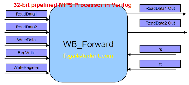
Verilog code for WB_Forward Unit:
`timescale 1 ps / 100 fs
// fpga4student.com: FPGA projects, Verilog Projects, VHDL projects
// Verilog project: 32-bit 5-stage Pipelined MIPS Processor in Verilog
// Write Back Forwarding
module WB_forward(ReadData1Out,ReadData2Out,ReadData1,ReadData2,rs,rt,WriteRegister,WriteData,RegWrite);
// WB Hazard: Reading data while writing
// Solve Hazard at the WriteBack Stage
output [31:0] ReadData1Out,ReadData2Out;
input [31:0] ReadData1,ReadData2,WriteData;
input [4:0] rs,rt,WriteRegister;
input RegWrite;
wire ReadSourceRs,ReadSourceRt;
wire compOut1,compOut2;
// behavior model
/*
always @(rs or rt or WriteRegister or WriteData or RegWrite)
begin
 if ((RegWrite==1)&&(WriteRegister != 0)&&(WriteRegister==rs))
  ReadSourceRs = 1'b1; //Forwarding WriteData to ReadData1
  else
  ReadSourceRs = 1'b0;
  if ((RegWrite==1)&&(WriteRegister != 0)&&(WriteRegister==rt))
  ReadSourceRt = 1'b1; //Forwarding WriteData to ReadData2
  else
  ReadSourceRt = 1'b0;
end
*/
// Structural model
or #(50) orWriteReg(orOut1,WriteRegister[4],WriteRegister[3],WriteRegister[2],WriteRegister[1],WriteRegister[0]);
CompareAddress Compare1(compOut1,WriteRegister,rs);
and #(50) andCondition1(ReadSourceRs,RegWrite,orOut1,compOut1);

CompareAddress Compare2(compOut2,WriteRegister,rt);
and #(50) andCondition2(ReadSourceRt,RegWrite,orOut1,compOut2);

mux2x32to32 muxReadData1( ReadData1Out,ReadData1,WriteData, ReadSourceRs);
mux2x32to32 muxReadData2( ReadData2Out,ReadData2,WriteData, ReadSourceRt);
endmodule
`timescale 1 ps / 100 fs
module CompareAddress(equal,Addr1,Addr2);
// fpga4student.com: FPGA projects, Verilog Projects, VHDL projects
// Verilog project: 32-bit 5-stage Pipelined MIPS Processor in Verilog
// Compare Address
output equal;
wire equal;
input [4:0] Addr1,Addr2;
wire [4:0] Addr1,Addr2,xorAddress;
xor #(50) xorAddress4(xorAddress[4],Addr1[4],Addr2[4]);
xor #(50) xorAddress3(xorAddress[3],Addr1[3],Addr2[3]);
xor #(50) xorAddress2(xorAddress[2],Addr1[2],Addr2[2]);
xor #(50) xorAddress1(xorAddress[1],Addr1[1],Addr2[1]);
xor #(50) xorAddress0(xorAddress[0],Addr1[0],Addr2[0]);
or #(50) Orgate1(OrAddr,xorAddress[4],xorAddress[3],xorAddress[2],xorAddress[1],xorAddress[0]);
not #(50) notgate1(equal,OrAddr);
endmodule
Now, we completed the Verilog code for all the necessary parts of the whole 32-bit pipelined MIPS Processor.
Let's go for the top level Verilog code of the 32-bit pipelined MIPS Processor:
`timescale 1 ps / 100 fs
// fpga4student.com: FPGA projects, Verilog Projects, VHDL projects
// Verilog project: 32-bit 5-stage Pipelined MIPS Processor in Verilog
// Top level Verilog code for 32-bit 5-stage Pipelined MIPS Processor
module MIPSpipeline(clk, reset);
input clk, reset;
wire [31:0] PC, PCin;
wire [31:0] PC4,ID_PC4,EX_PC4;
wire [31:0] PCbne,PC4bne,PCj,PC4bnej,PCjr; // PC signals in MUX
wire [31:0] Instruction,ID_Instruction,EX_Instruction; // Output of Instruction Memory
wire [5:0] Opcode,Function; // Opcode, Function

// Extend
wire [15:0] imm16; // immediate in I type instruction
wire [31:0] Im16_Ext,EX_Im16_Ext;
wire [31:0] sign_ext_out,zero_ext_out;
// regfile
wire [4:0] rs,rt,rd,EX_rs,EX_rt,EX_rd,EX_WriteRegister,MEM_WriteRegister,WB_WriteRegister;
wire [31:0] WB_WriteData, ReadData1, ReadData2,ReadData1Out,ReadData2Out, EX_ReadData1, EX_ReadData2;

// ALU
wire [31:0] Bus_A_ALU,Bus_B_ALU,Bus_B_forwarded;
wire [31:0] EX_ALUResult,MEM_ALUResult,WB_ALUResult;
wire ZeroFlag, OverflowFlag, CarryFlag, NegativeFlag,notZeroFlag;

wire [31:0] WriteDataOfMem,MEM_ReadDataOfMem,WB_ReadDataOfMem;

//Control signals
wire RegDst,ALUSrc,MemtoReg,RegWrite,MemRead,MemWrite,Branch,Jump,SignZero,JRControl;
wire ID_RegDst,ID_ALUSrc,ID_MemtoReg,ID_RegWrite,ID_MemRead,ID_MemWrite,ID_Branch,ID_JRControl;
wire EX_RegDst,EX_ALUSrc,EX_MemtoReg,EX_RegWrite,EX_MemRead,EX_MemWrite,EX_Branch,EX_JRControl;
wire MEM_MemtoReg,MEM_RegWrite,MEM_MemRead,MEM_MemWrite;
wire WB_MemtoReg,WB_RegWrite;
wire [1:0] ALUOp,ID_ALUOp,EX_ALUOp;
wire [1:0] ALUControl;
wire bneControl,notbneControl;
wire JumpControl,JumpFlush;
wire [1:0] ForwardA,ForwardB;
    //flush
wire IF_flush,IFID_flush,notIFID_flush,Stall_flush,flush;
//shift left
wire [31:0] shiftleft2_bne_out,shiftleft2_jump_out; // shift left output
// PC Write Enable, IF/ID Write Enable
wire PC_WriteEn,IFID_WriteEn;


//====== PC register======
register PC_Reg(PC,PCin,PC_WriteEn,reset,clk);
Add Add1(PC4,PC,{29'b0,3'b100}); // PC4 = PC + 4

InstructionMem InstructionMem1(Instruction, PC);

// register IF/ID

register IFID_PC4(ID_PC4,PC4,IFID_WriteEn,reset,clk);
register IFID_Instruction(ID_Instruction,Instruction,IFID_WriteEn,reset,clk);
RegBit IF_flush_bit(IFID_flush,IF_flush, IFID_WriteEn,reset, clk);

//========= ID STAGE===========
assign Opcode = ID_Instruction[31:26];
assign Function = ID_Instruction[5:0];
assign rs = ID_Instruction[25:21];
assign rt = ID_Instruction[20:16];
assign rd = ID_Instruction[15:11];
assign imm16= ID_Instruction[15:0];

 // Main Control
Control MainControl(
RegDst,
ALUSrc,
MemtoReg,
RegWrite,
MemRead,
MemWrite,
Branch,
ALUOp,
Jump,
SignZero,
Opcode
);

 // Regfile
regfile Register_File(
ReadData1,
ReadData2,
WB_WriteData,
rs,
rt,
WB_WriteRegister,
WB_RegWrite,
reset,
clk);

// forward Read Data if Write and Read at the same time
WB_forward  WB_forward_block(ReadData1Out,ReadData2Out,ReadData1,ReadData2,rs,rt,WB_WriteRegister,WB_WriteData,WB_RegWrite);
 // Sign-extend
sign_extend sign_extend1(sign_ext_out,imm16);
 // Zero-extend
zero_extend zero_extend1(zero_ext_out,imm16);
 // immediate extend: sign or zero
mux2x32to32 muxSignZero( Im16_Ext,sign_ext_out,zero_ext_out, SignZero);

JRControl_Block JRControl_Block1( JRControl, ALUOp, Function);

Discard_Instr Discard_Instr_Block(ID_flush,IF_flush,JumpControl,bneControl,EX_JRControl);

or #(50) OR_flush(flush,ID_flush,IFID_flush,Stall_flush);
flush_block flush_block1(ID_RegDst,ID_ALUSrc,ID_MemtoReg,ID_RegWrite,ID_MemRead,ID_MemWrite,ID_Branch,ID_ALUOp,
ID_JRControl,flush,RegDst,ALUSrc,MemtoReg,RegWrite,MemRead,MemWrite,Branch,ALUOp,JRControl);

//==========EX STAGE=========================
// thanh ghi ID/EX
register IDEX_PC4(EX_PC4,ID_PC4,1'b1,reset,clk);

register IDEX_ReadData1(EX_ReadData1,ReadData1Out,1'b1,reset,clk);
register IDEX_ReadData2(EX_ReadData2,ReadData2Out,1'b1,reset,clk);


register IDEX_Im16_Ext(EX_Im16_Ext,Im16_Ext,1'b1,reset,clk);
register IDEX_rs_rt_rd(EX_Instruction[31:0],ID_Instruction,1'b1,reset,clk);
assign EX_rs = EX_Instruction[25:21];
assign EX_rt = EX_Instruction[20:16];
assign EX_rd = EX_Instruction[15:11];
// 9 control signals via ID/EX
RegBit  IDEX_RegDst(EX_RegDst, ID_RegDst, 1'b1,reset, clk);
RegBit  IDEX_ALUSrc(EX_ALUSrc, ID_ALUSrc, 1'b1,reset, clk);
RegBit  IDEX_MemtoReg(EX_MemtoReg, ID_MemtoReg, 1'b1,reset, clk);
RegBit  IDEX_RegWrite(EX_RegWrite, ID_RegWrite, 1'b1,reset, clk);
RegBit  IDEX_MemRead(EX_MemRead, ID_MemRead, 1'b1,reset, clk);
RegBit  IDEX_MemWrite(EX_MemWrite, ID_MemWrite, 1'b1,reset, clk);
RegBit  IDEX_Branch(EX_Branch, ID_Branch, 1'b1,reset, clk);
RegBit  IDEX_JRControl(EX_JRControl, ID_JRControl, 1'b1,reset, clk);
RegBit  IDEX_ALUOp1(EX_ALUOp[1], ID_ALUOp[1], 1'b1,reset, clk);
RegBit  IDEX_ALUOp0(EX_ALUOp[0], ID_ALUOp[0], 1'b1,reset, clk);
//  Forwarding unit
ForwardingUnit Forwarding_Block(ForwardA,ForwardB,MEM_RegWrite,WB_RegWrite,MEM_WriteRegister,WB_WriteRegister,EX_rs,EX_rt);
// mux 3 x32 to 32 to choose source of ALU (forwarding)
mux3x32to32  mux3A(Bus_A_ALU,EX_ReadData1,MEM_ALUResult,WB_WriteData,ForwardA);
mux3x32to32  mux3B(Bus_B_forwarded,EX_ReadData2,MEM_ALUResult,WB_WriteData,ForwardB);
// mux 2x32 to 32 to select source Bus B of ALU
mux2x32to32 muxALUSrc( Bus_B_ALU,Bus_B_forwarded,EX_Im16_Ext, EX_ALUSrc);
// ALU Control
ALUControl_Block ALUControl_Block1( ALUControl, EX_ALUOp, EX_Im16_Ext[5:0]);
// EX_Im16_Ext[5:0] is function

// ALU
alu alu_block(EX_ALUResult, CarryFlag, ZeroFlag, OverflowFlag, NegativeFlag, Bus_A_ALU, Bus_B_ALU, ALUControl);

// mux 2x5 to 5 choose shift register is Rd or Rt
mux2x5to5 muxRegDst( EX_WriteRegister,EX_rt,EX_rd, EX_RegDst);

//==============MEM STAGE=================
// register EX/MEM
register EXMEM_ALUResult(MEM_ALUResult,EX_ALUResult,1'b1,reset,clk);
register EXMEM_WriteDataOfMem(WriteDataOfMem, Bus_B_forwarded,1'b1,reset,clk);
RegBit  EXMEM_MemtoReg(MEM_MemtoReg, EX_MemtoReg, 1'b1,reset, clk);
RegBit  EXMEM_RegWrite(MEM_RegWrite, EX_RegWrite, 1'b1,reset, clk);
RegBit  EXMEM_MemRead(MEM_MemRead, EX_MemRead, 1'b1,reset, clk);
RegBit  EXMEM_MemWrite(MEM_MemWrite, EX_MemWrite, 1'b1,reset, clk);
RegBit  EXMEM_WriteRegister4(MEM_WriteRegister[4], EX_WriteRegister[4], 1'b1,reset, clk);
RegBit  EXMEM_WriteRegister3(MEM_WriteRegister[3], EX_WriteRegister[3], 1'b1,reset, clk);
RegBit  EXMEM_WriteRegister2(MEM_WriteRegister[2], EX_WriteRegister[2], 1'b1,reset, clk);
RegBit  EXMEM_WriteRegister1(MEM_WriteRegister[1], EX_WriteRegister[1], 1'b1,reset, clk);
RegBit  EXMEM_WriteRegister0(MEM_WriteRegister[0], EX_WriteRegister[0], 1'b1,reset, clk);

 // Data Memory
dataMem dataMem1(MEM_ReadDataOfMem, //data
     MEM_ALUResult,       //address
     WriteDataOfMem,       //writedata
     MEM_MemWrite,        //writeenable
     MEM_MemRead,
     clk);
//==========WB STAGE====================
// register MEM/WB
register MEMWB_ReadDataOfMem(WB_ReadDataOfMem,MEM_ReadDataOfMem,1'b1,reset,clk);
register MEMWB_ALUResult(WB_ALUResult,MEM_ALUResult,1'b1,reset,clk);
RegBit  MEMWB_WriteRegister4(WB_WriteRegister[4], MEM_WriteRegister[4], 1'b1,reset, clk);
RegBit  MEMWB_WriteRegister3(WB_WriteRegister[3], MEM_WriteRegister[3], 1'b1,reset, clk);
RegBit  MEMWB_WriteRegister2(WB_WriteRegister[2], MEM_WriteRegister[2], 1'b1,reset, clk);
RegBit  MEMWB_WriteRegister1(WB_WriteRegister[1], MEM_WriteRegister[1], 1'b1,reset, clk);
RegBit  MEMWB_WriteRegister0(WB_WriteRegister[0], MEM_WriteRegister[0], 1'b1,reset, clk);

RegBit  MEMWB_MemtoReg(WB_MemtoReg, MEM_MemtoReg, 1'b1,reset, clk);
RegBit  MEMWB_RegWrite(WB_RegWrite, MEM_RegWrite, 1'b1,reset, clk);

 // Select Data to WriteData for regfile
mux2x32to32 muxMemtoReg( WB_WriteData, WB_ALUResult, WB_ReadDataOfMem,WB_MemtoReg);

//Stalling
StallControl StallControl_block(PC_WriteEn,IFID_WriteEn,Stall_flush,EX_MemRead,EX_rt,rs,rt,Opcode);

//Jump,bne, JRs
 // bne: Branch if not equal
shift_left_2 shiftleft2_bne(shiftleft2_bne_out, EX_Im16_Ext);
Add Add_bne(PCbne,EX_PC4,shiftleft2_bne_out);
not #(50) notZero(notZeroFlag,ZeroFlag);
and #(50) andbneControl(bneControl,EX_Branch,notZeroFlag);
mux2x32to32  muxbneControl( PC4bne,PC4, PCbne, bneControl);
  // jump
shift_left_2 shiftleft2_jump(shiftleft2_jump_out, {6'b0,ID_Instruction[25:0]});
assign PCj = {ID_PC4[31:28],shiftleft2_jump_out[27:0]};

not #(50) notIFIDFlush(notIFID_flush,IFID_flush);
and #(50) andJumpFlush(JumpFlush,Jump,notIFID_flush);
not #(50) notbne(notbneControl,bneControl);
and #(50) andJumpBNE(JumpControl,JumpFlush,notbneControl);
mux2x32to32  muxJump( PC4bnej,PC4bne, PCj, JumpControl);

 // JR: Jump Register
assign PCjr = Bus_A_ALU;
mux2x32to32  muxJR( PCin,PC4bnej, PCjr, EX_JRControl);

endmodule
Verilog Testbench code for the 32-bit pipelined MIPS Processor:
`timescale 1 ps / 100 fs
module MIPSStimulus();
// fpga4student.com: FPGA projects, Verilog Projects, VHDL projects
// Verilog project: 32-bit 5-stage Pipelined MIPS Processor in Verilog
// Testbench Verilog code for 32-bit 5-stage Pipelined MIPS Processor
parameter ClockDelay = 5000;

reg clk,reset;


MIPSpipeline  myMIPS(clk, reset);
initial clk = 0;
always #(ClockDelay/2) clk = ~clk;

initial
begin
   reset = 1;
  #(ClockDelay/4);
  reset = 0;
end
endmodule
To verify the operation of the pipelined MIPS processor, I created a piece of instructions which includes all the data and control hazards. The instructions are added to the instruction memory as shown in the following figure and then, run simulation in Modelsim.

It is noted that the instructions need to be converted into binary data and saved in the "instr.txt" file. I converted the above sample instructions into binary data and provided in part 1.
After that, just run the simulation in Modelsim, and check the simulation waveform and memory editor as well. Below are the correct simulation waveform in 24 clock cycles.
 |
| Simulation waveform for the first 12 cycles |
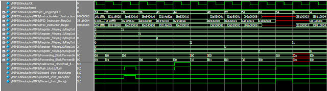 |
| Simulation waveform for the next 12 cycles |
Leave a comment if you have any confusion or difficulty in simulation.
It is noted that you need to go through all the necessary parts( Part 1, Part 2, and Part 3) to fully understand the process of designing the pipelined MIPS processor, and collect all the required Verilog code to be able to run the pipelined MIPS processor in simulation.
You may like this:Verilog code for a Microcontroller
A complete 8-bit Microcontroller in VHDL
Single-cycle MIPS Processor in Verilog
Verilog Code for 16-bit RISC Processor
VHDL code for MIPS Processor
What is FPGA Programming? FPGA vs Software programming
Recommended and affordable Xilinx FPGA boards for students
Recommended and affordable Altera FPGA boards for students
Recommended Verilog projects:
2. Verilog code for FIFO memory
3. Verilog code for 16-bit single-cycle MIPS processor
4. Programmable Digital Delay Timer in Verilog HDL
5. Verilog code for basic logic components in digital circuits
6. Verilog code for 32-bit Unsigned Divider
7. Verilog code for Fixed-Point Matrix Multiplication
8. Plate License Recognition in Verilog HDL
9. Verilog code for Carry-Look-Ahead Multiplier
10. Verilog code for a Microcontroller
11. Verilog code for 4x4 Multiplier
12. Verilog code for Car Parking System
13. Image processing on FPGA using Verilog HDL
14. How to load a text file into FPGA using Verilog HDL
15. Verilog code for Traffic Light Controller
16. Verilog code for Alarm Clock on FPGA
17. Verilog code for comparator design
18. Verilog code for D Flip Flop
19. Verilog code for Full Adder
20. Verilog code for counter with testbench
21. Verilog code for 16-bit RISC Processor
22. Verilog code for button debouncing on FPGA
23. How to write Verilog Testbench for bidirectional/ inout ports
24. Tic Tac Toe Game in Verilog and LogiSim
25. 32-bit 5-stage Pipelined MIPS Processor in Verilog (Part-1)
26. 32-bit 5-stage Pipelined MIPS Processor in Verilog (Part-2)
27. 32-bit 5-stage Pipelined MIPS Processor in Verilog (Part-3)
30. N-bit Adder Design in Verilog25. 32-bit 5-stage Pipelined MIPS Processor in Verilog (Part-1)
26. 32-bit 5-stage Pipelined MIPS Processor in Verilog (Part-2)
27. 32-bit 5-stage Pipelined MIPS Processor in Verilog (Part-3)
31. Verilog vs VHDL: Explain by Examples
32. Verilog code for Clock divider on FPGA
33. How to generate a clock enable signal in Verilog
34. Verilog code for PWM Generator
35. Verilog coding vs Software Programming
36. Verilog code for Sequence Detector using Moore FSM


It is noted that the instructions need to be converted into binary data and saved in the "instr.txt"
ReplyDeleteWhen I simulate, modelsim show me memory filled with xxxxxxxxxxxxxxxxx (dont care), it looks like isn't loading anything to the memory.I don't know what I'm doing wrong. Likely isnt the dispossition of the numbers in the .txt file. Maybe is because I'm intending to load file with $readmemb in another module which is not testbench?
If you want to initialize the content of the data memory, create the "data.dat" file and add the readmem command to the data memory code to initialize it.
DeleteRun the simulation for some time to see the results. Make sure you understand the instructions in the "instr.txt" file.
I didn't see the PC module, so what about that ?
ReplyDeletehttp://www.fpga4student.com/2017/06/32-bit-pipelined-mips-processor-in-verilog-1.html
DeleteIt is provided in part 1 of the Pipelined MIPS processor.
In datamemory module, I saw the $readmemh("data.dat".....), so what is the purpose of this ?, can you explain it for me ?
DeleteIt was commented already. It is used for reading data memory from a .dat file, just in case that you want to enter the memory content from .dat or .txt file to the data memory.
DeleteI want to add exception and interupts into this cpu, what should I do from the beginning
ReplyDeleteI want to know.You did about exception or interrupt ? You can help me. Thank you
Deletemy waveform is not the same, it only has 3 entries. clk, reset and clockdelay. what's the reason?
ReplyDeleteCan some one give the data.dat file format for the given program and instructions
ReplyDelete