

In this project, Verilog code for a microcontroller is presented. The microcontroller architecture and instruction set are shown in part 1 and part 2.

First is the Verilog code for ALU unit:
// fpga4student.com: FPGA project, Verilog project, VHDL project
// Verilog project: Verilog code for Microcontroller
// Verilog code for ALU
module ALU(  input [7:0] Operand1,Operand2,
  input E,
  input [3:0] Mode,
  input [3:0] CFlags,
  output  [7:0] Out,
  output  [3:0] Flags
// the Z (zero), C (carry), S (sign),O (overflow) bits, from MSB to LSB, connected to status register
   );
  wire Z,S,O;
  reg CarryOut;
  reg [7:0] Out_ALU;
  always @(*)
  begin
  case(Mode)
  4'b0000: {CarryOut,Out_ALU} = Operand1 + Operand2;
  4'b0001: begin Out_ALU = Operand1 -  Operand2;
  CarryOut = !Out_ALU[7];
  end
  4'b0010: Out_ALU = Operand1;
  4'b0011: Out_ALU = Operand2;
  4'b0100: Out_ALU = Operand1 & Operand2;
  4'b0101: Out_ALU = Operand1 | Operand2;
  4'b0110: Out_ALU = Operand1 ^ Operand2;
  4'b0111: begin
  Out_ALU = Operand2 - Operand1;
  CarryOut = !Out_ALU[7];
  end
  4'b1000: {CarryOut,Out_ALU} = Operand2 + 8'h1;
  4'b1001: begin
  Out_ALU = Operand2 - 8'h1;
  CarryOut = !Out_ALU[7];
  end
  4'b1010: Out_ALU = (Operand2 << Operand1[2:0])| ( Operand2 >> Operand1[2:0]);
  4'b1011: Out_ALU = (Operand2 >> Operand1[2:0])| ( Operand2 << Operand1[2:0]);
  4'b1100: Out_ALU = Operand2 << Operand1[2:0];
  4'b1101: Out_ALU = Operand2 >> Operand1[2:0];
  4'b1110: Out_ALU = Operand2 >>> Operand1[2:0];
  4'b1111: begin
 Out_ALU = 8'h0 - Operand2;
 CarryOut = !Out_ALU[7];
 end
 default: Out_ALU = Operand2;
 endcase
 end
 assign O = Out_ALU[7] ^ Out_ALU[6];
 assign Z = (Out_ALU == 0)? 1'b1 : 1'b0;
 assign S = Out_ALU[7];
 assign Flags = {Z,CarryOut,S,O};
 assign Out = Out_ALU;
// fpga4student.com: FPGA project, Verilog project, VHDL project
endmodule
Next is the Verilog code for data memory:
// fpga4student.com: FPGA project, Verilog project, VHDL project
// Verilog project: Verilog code for Microcontroller
// Verilog code for data memory
 module DMem( input clk,
     input E, // Enable port
     input WE, // Write enable port
     input [3:0] Addr, // Address port
     input [7:0] DI, // Data input port
     output [7:0] DO // Data output port
    );
reg [7:0] data_mem [255:0];
// fpga4student.com: FPGA project, Verilog project, VHDL project
always @(posedge clk)
begin
 if(E==1 && WE ==1)
  data_mem[Addr] <= DI;
end
 assign DO = (E ==1 )? data_mem[Addr]:0;
endmodule
// Verilog project: Verilog code for microcontroller
// Submodule: Verilog code for Adder and MUXs
module adder( input [7:0] In,
      output [7:0] Out
    );

assign Out = In + 1;

endmodule
module MUX1( input [7:0] In1,In2,
     input Sel,
     output [7:0] Out
    );

assign Out = (Sel==1)? In1: In2;
endmodule
Continue on the Verilog code for program memory:
// Verilog project: Verilog code for microcontroller
// Submodule: Verilog code for Adder and MUXs// fpga4student.com: FPGA project, Verilog project, VHDL project
// Verilog project: Verilog code for microcontroller
module PMem( input clk,
   input E, // Enable port
  input [7:0] Addr, // Address port
  output [11:0] I, // Instruction port
  // 3 special ports are used to load program to the memory
  input LE, // Load enable port
  input[7:0] LA, // Load address port
  input [11:0] LI//Load instruction port
   );
 reg [11:0] Prog_Mem[255:0] ;
// fpga4student.com: FPGA project, Verilog project, VHDL project
always @(posedge clk)
 begin
 if(LE == 1) begin
 Prog_Mem[LA] <= LI;
 end
 end
 assign I =  (E == 1) ?  Prog_Mem[Addr]: 0 ;
endmodule
module adder( input [7:0] In,
      output [7:0] Out
    );

assign Out = In + 1;

endmodule
module MUX1( input [7:0] In1,In2,
     input Sel,
     output [7:0] Out
    );

assign Out = (Sel==1)? In1: In2;
endmodule
Next, the Verilog code for Control unit:
// fpga4student.com: FPGA project, Verilog project, VHDL project
// Verilog project: Verilog code for microcontroller
// Control unit in Verilog
module Control_Logic( input[1:0] stage,
  input [11:0] IR,
  input [3:0] SR,
 output  reg PC_E,Acc_E,SR_E,IR_E,DR_E,PMem_E,DMem_E,DMem_WE,ALU_E,MUX1_Sel,MUX2_Sel,PMem_LE,
  output reg [3:0] ALU_Mode
    );
 parameter LOAD = 2'b00,FETCH = 2'b01, DECODE = 2'b10, EXECUTE = 2'b11;
 always @(*)
 begin
 PMem_LE = 0;
 PC_E = 0;
 Acc_E = 0;
 SR_E = 0;
 IR_E = 0;
 DR_E = 0;
 PMem_E = 0;
 DMem_E = 0;
 DMem_WE = 0;
 ALU_E  =0;
 ALU_Mode = 4'd0;
 MUX1_Sel = 0;
 MUX2_Sel = 0;
 if(stage== LOAD )
 begin
 PMem_LE = 1;
 PMem_E = 1;
 end
 else if(stage== FETCH ) begin
 IR_E = 1;
 PMem_E = 1;
 end
 else if(stage== DECODE ) begin
 if( IR[11:9] == 3'b001)
 begin
 DR_E = 1;
 DMem_E = 1;
 end
 else
 begin
 DR_E = 0;
 DMem_E = 0;
 end
 end
 else if(stage== EXECUTE )
 begin
 if(IR[11]==1) begin // ALU I-type
 PC_E = 1;
 Acc_E = 1;
 SR_E = 1;
 ALU_E = 1;
 ALU_Mode = IR[10:8];
 MUX1_Sel = 1;
 MUX2_Sel = 0;
 end
 else if(IR[10]==1) // JZ, JC,JS, JO
 begin
 PC_E = 1;
 MUX1_Sel = SR[IR[9:8]];
 end
 else if(IR[9]==1)
 begin
 PC_E = 1;
 Acc_E = IR[8];
 SR_E = 1;
 DMem_E = !IR[8];
 DMem_WE = !IR[8];
 ALU_E = 1;
 ALU_Mode = IR[7:4];
 MUX1_Sel = 1;
 MUX2_Sel = 1;
 end
 else if(IR[8]==0)
 begin
 PC_E = 1;
 MUX1_Sel = 1;
 end
 else
 begin
 PC_E = 1;
 MUX1_Sel = 0;
 end
 end
 end
endmodule
Finally, the Verilog code for microcontroller:
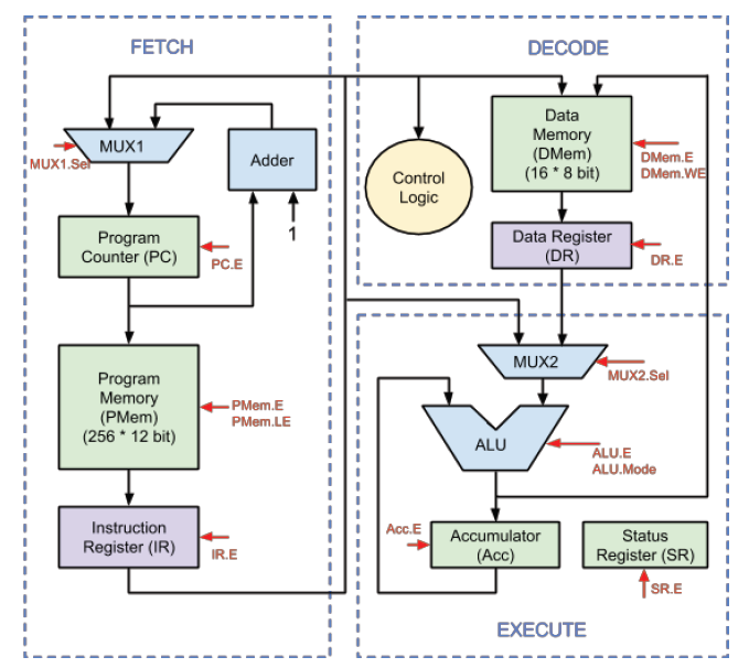
// The microcontroller (similar to Microchip PIC12, simplified extensively, not compatible in
// instruction set) in this project is a 3 cycle nonpipeline
// 8 bit Harvard structure microcontroller, illustrated as the following block diagram
// fpga4student.com: FPGA project, Verilog project, VHDL project
// Verilog project: Verilog code for microcontroller
module MicroController(input clk,rst
    );
  parameter LOAD = 2'b00,FETCH = 2'b01, DECODE = 2'b10, EXECUTE = 2'b11;
  reg [1:0] current_state,next_state;
  reg [11:0] program_mem[9:0];
  reg load_done;
  reg[7:0] load_addr;
  wire[11:0] load_instr;
  reg[7:0] PC,  DR, Acc;
  reg [11:0] IR;
  reg [3:0]  SR;
  wire PC_E,Acc_E,SR_E,DR_E,IR_E;
 reg PC_clr,Acc_clr,SR_clr,DR_clr,IR_clr;
 wire [7:0] PC_updated,DR_updated;
 wire[11:0] IR_updated;
 wire[3:0] SR_updated;
 wire PMem_E,DMem_E,DMem_WE,ALU_E,PMem_LE,MUX1_Sel,MUX2_Sel;
 wire [3:0] ALU_Mode;
 wire [7:0] Adder_Out;
 wire [7:0] ALU_Out,ALU_Oper2;
 // LOAD instruction memory
 initial
 begin
 $readmemb("program_mem.dat", program_mem,0,9);
 end
 // ALU
 ALU ALU_unit( .Operand1(Acc),
      .Operand2(ALU_Oper2),
   .E(ALU_E),
   .Mode(ALU_Mode),
   .CFlags(SR),
      .Out(ALU_Out),
      .Flags(SR_updated) // the Z (zero), C (carry), S (sign),O (overflow) bits, from MSB to LSB, connected to status register
  );
 // MUX2
 MUX1 MUX2_unit( .In2(IR[7:0]),.In1(DR),
  .Sel(MUX2_Sel),
  .Out(ALU_Oper2)
    );
 // Data Memory
 DMem DMem_unit( .clk(clk),
  .E(DMem_E), // Enable port
  .WE(DMem_WE), // Write enable port
  .Addr(IR[3:0]), // Address port
  .DI(ALU_Out), // Data input port
  .DO(DR_updated) // Data output port
    );
 // Program memory
 PMem PMem_unit( .clk(clk),
  .E(PMem_E), // Enable port
  .Addr(PC), // Address port
  .I(IR_updated), // Instruction port
  // 3 special ports are used to load program to the memory
  .LE(PMem_LE), // Load enable port
  .LA(load_addr), // Load address port
  .LI(load_instr)//Load instruction port
   );
 // PC ADder
 adder PC_Adder_unit( .In(PC),
   .Out(Adder_Out)
    );
// fpga4student.com: FPGA project, Verilog project, VHDL project
// MUX1
 MUX1 MUX1_unit( .In2(IR[7:0]),.In1(Adder_Out),
  .Sel(MUX1_Sel),
  .Out(PC_updated)
    );
 // Control logic
 Control_Logic Control_Logic_Unit( .stage(current_state),
  .IR(IR),
  .SR(SR),
  .PC_E(PC_E),
  .Acc_E(Acc_E),
  .SR_E(SR_E),
  .IR_E(IR_E),
  .DR_E(DR_E),
  .PMem_E(PMem_E),
  .DMem_E(DMem_E),
  .DMem_WE(DMem_WE),
  .ALU_E(ALU_E),
  .MUX1_Sel(MUX1_Sel),
  .MUX2_Sel(MUX2_Sel),
  .PMem_LE(PMem_LE),
  .ALU_Mode(ALU_Mode)
    );
// fpga4student.com: FPGA project, Verilog project, VHDL project
 // LOAD
 always @(posedge clk)
 begin
 if(rst==1) begin
 load_addr <= 0;
 load_done <= 1'b0;
 end
 else if(PMem_LE==1)
 begin
 load_addr <= load_addr + 8'd1;
 if(load_addr == 8'd9)
 begin
 load_addr <= 8'd0;
 load_done <= 1'b1;
 end
 else
 begin
 load_done <= 1'b0;
 end
 end
 end
// fpga4student.com: FPGA project, Verilog project, VHDL project
 assign load_instr = program_mem[load_addr];
 // next state
 always @(posedge clk)
 begin
 if(rst==1)
 current_state <= LOAD;
 else
 current_state <= next_state;
 end
 always @(*)
 begin
 PC_clr = 0;
 Acc_clr = 0;
 SR_clr = 0;
 DR_clr = 0;
 IR_clr = 0;
 case(current_state)
 LOAD: begin
 if(load_done==1) begin
 next_state = FETCH;
 PC_clr = 1;
 Acc_clr = 1;
 SR_clr = 1;
 DR_clr = 1;
 IR_clr = 1;
 end
 else
 next_state = LOAD;
 end
 FETCH: begin
 next_state = DECODE;
 end
 DECODE: begin
 next_state = EXECUTE;
 end
 EXECUTE: begin
 next_state = FETCH;
 end
 endcase
 end
// fpga4student.com: FPGA project, Verilog project, VHDL project
 // 3 programmer visible register
 always @(posedge clk)
 begin
 if(rst==1)
 begin
 PC <= 8'd0;
 Acc <= 8'd0;
 SR <= 4'd0;
 end
 else
 begin
 if(PC_E==1'd1)
 PC <= PC_updated;
 else if (PC_clr==1)
 PC <= 8'd0;
 if(Acc_E==1'd1)
 Acc <= ALU_Out;
 else if (Acc_clr==1)
 Acc <= 8'd0;
 if(SR_E==1'd1)
 SR <= SR_updated;
 else if (SR_clr==1)
 SR <= 4'd0;
 end
 end
// fpga4student.com: FPGA project, Verilog project, VHDL project
 // 2 programmer invisible register
 always @(posedge clk)
 begin
 if(DR_E==1'd1)
 DR <= DR_updated;
 else if (DR_clr==1)
 DR  <= 8'd0;
 if(IR_E==1'd1)
 IR <= IR_updated;
 else if(IR_clr==1)
 IR <= 12'd0;
 end
endmodule
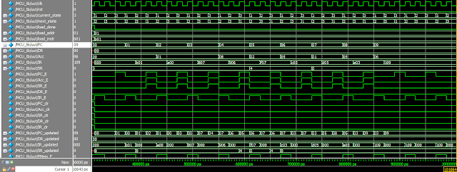
Verilog testbench code to verify the microcontroller:
module MCU_tb;
// fpga4student.com: FPGA project, Verilog project, VHDL project
// Verilog project: Verilog code for microcontroller
// Inputs
reg clk;
reg rst;
// Instantiate the Unit Under Test (UUT)
MicroController uut (
.clk(clk),
.rst(rst)
);
initial begin
// Initialize Inputs
rst = 1;
// Wait 100 ns for global reset to finish
#100;
rst = 0;
end
initial begin
clk = 0;
forever #10 clk = ~clk;
end
endmodule
Test program 1:
0000_0000_0000
1011_0000_0001
0010_0010_0000
1011_0000_0000
0011_0011_0000
0001_0000_0101
0000_0000_0000
0000_0000_0000
0000_0000_0000
0000_0000_0000
Test program 2:
0000_0000_0000
1011_0000_0001
0010_0010_0000
0011_0000_0000
0010_0000_0000
0011_0001_0000
0010_0001_0000
0011_0111_0000
0010_0111_0000
0001_0000_1001
Test program 3:
0000_0000_0000
1011_0000_0101
0010_0010_0000
0010_0010_0001
0010_0010_0010
1011_0000_0011
0010_0100_0000
0010_0101_0001
0010_0110_0010
0001_0000_1001
Test program 4:
0000_0000_0000
1011_0000_0101
1010_0000_0000
1000_0000_0111
1001_0000_0110
1111_0000_0111
1100_0000_0011
1101_0000_0101
1110_0000_0011
0001_0000_1001
Use the four test program to run simulation and check if the microcontroller is working correctly.
Recommended Verilog projects:
2. Verilog code for FIFO memory
3. Verilog code for 16-bit single-cycle MIPS processor
4. Programmable Digital Delay Timer in Verilog HDL
5. Verilog code for basic logic components in digital circuits
6. Verilog code for 32-bit Unsigned Divider
7. Verilog code for Fixed-Point Matrix Multiplication
8. Plate License Recognition in Verilog HDL
9. Verilog code for Carry-Look-Ahead Multiplier
10. Verilog code for a Microcontroller
11. Verilog code for 4x4 Multiplier
12. Verilog code for Car Parking System
13. Image processing on FPGA using Verilog HDL
14. How to load a text file into FPGA using Verilog HDL
15. Verilog code for Traffic Light Controller
16. Verilog code for Alarm Clock on FPGA
17. Verilog code for comparator design
18. Verilog code for D Flip Flop
19. Verilog code for Full Adder
20. Verilog code for counter with testbench
21. Verilog code for 16-bit RISC Processor
22. Verilog code for button debouncing on FPGA
23. How to write Verilog Testbench for bidirectional/ inout ports
24. Tic Tac Toe Game in Verilog and LogiSim
25. 32-bit 5-stage Pipelined MIPS Processor in Verilog (Part-1)
26. 32-bit 5-stage Pipelined MIPS Processor in Verilog (Part-2)
27. 32-bit 5-stage Pipelined MIPS Processor in Verilog (Part-3)
28. Verilog code for Decoder25. 32-bit 5-stage Pipelined MIPS Processor in Verilog (Part-1)
26. 32-bit 5-stage Pipelined MIPS Processor in Verilog (Part-2)
27. 32-bit 5-stage Pipelined MIPS Processor in Verilog (Part-3)
29. Verilog code for Multiplexers
30. N-bit Adder Design in Verilog
31. Verilog vs VHDL: Explain by Examples
32. Verilog code for Clock divider on FPGA
33. How to generate a clock enable signal in Verilog
34. Verilog code for PWM Generator
35. Verilog coding vs Software Programming
36. Verilog code for Moore FSM Sequence Detector
37. Verilog code for 7-segment display controller on Basys 3 FPGA


Nice but following modules are missing:
ReplyDelete-MUX1
-adder
Updated, thanks.
DeleteAlso can you please detail the instruction set ? I sucessfully synthetized your code for a altera cyclone IV, but didn't run it right now, I'm trying to understand the purpose of the first test program, looks like a counter or something like that
ReplyDeleteInstruction set: http://www.fpga4student.com/2016/11/verilog-hdl-implementation-of-micro.html
ReplyDeleteArchitecture Design: http://www.fpga4student.com/2016/11/verilog-microcontroller-code.html
Thanks !
DeleteSir, i want to add one MMIO 8 bit PortA, to this microntroller (say at aadress 0x08 of DRAM) exactely as is done in every micrcontroller, so that it is possible to read or write to uC PORT using its address only. So, pls suggest possible changesbin the code.
ReplyDeleteYou can refer to this: http://www.fpga4student.com/2016/12/a-complete-8-bit-microcontroller-in-vhdl.html
ReplyDeleteIn this microcontroller, memory and IO are added as you want.
Sir, can u please share "program_mem.dat" u hv mentioned in $readmemb.
ReplyDeleteThe test program are there. Test program 1 -> 4. Copy it into the program_mem.dat.
DeleteI am not able to simulate it properly. Could you please help me with the test program? Also, the simulation shows only 2 elements - clock and reset. Please help.
ReplyDelete$readmemb("program_mem.dat", program_mem,0,9);
DeleteYou need to load different test program into the "program_mem.dat" file and run simulation. Yes, only clock and reset provided, but you need to look at the simulation waveform and data memory to see the operation of the MCU.
I am using Xilinx ISE 14.7, I have created the txt file copied the contents of "test program 1" into it and renamed it to "program_mem.dat", and then tried to simulate. From where can shall I see the results?
DeleteAdd necessary signals to simulation waveform to see the results. You need to understand the program which is stored in the instruction memory so that you can understand the results on simulation waveform
DeleteCan you please upload the "program_mem.dat" file? I have error when simulate the above code for progran_mem.dat file.Can you please tell me how do i simulate with that dat file.
ReplyDeleteThank you
You need to create this file and copy the provided test program to the file "program_mem.dat" which you created. Then, run simulation and see results on simulation waveform.
DeleteI created a text file, renamed it "program_mem.dat". Then copied one of the test program to it and then saved the text file in the folder where my verilog files are being saved. Still it is showing error that file cannot be found. Please help
ReplyDeleteSave the file into the same folder that you run the code. The file should be named "program_mem.dat" not "program_mem.dat.txt".
DeleteThanks. It works fine now. Just one more question, this is a 12 bit Microcontroller right or 8 bit Microcontroller?
DeleteHello,can you help me too ? I am also facing the same probem. It is the showing the file cannot be found.
DeleteIn Control Unit
ReplyDeleteelse if(IR[8]==0) //// This should be else if (IR[8]==1)? I guess or Is it correct?
begin
PC_E = 1;
MUX1_Sel = 1;
end
else
begin
PC_E = 1;
MUX1_Sel = 0;
end
end
end
endmodule
Nope. The code were already correct. IR[8]==1 => MUX1_Sel=0 to select IR[7:0] for jump or branch instructions (IR[8]=1). Otherwise (IR[8]==0), MUX1_Sel=1 to increase PC by 1 (Adder_Out). Check the MUX1 code.
Deletewill this code execute in VIVADO 2017.4
ReplyDeleteSure. You can use Vivado for this project.
Deletewhat are the inputs i have to give in the test bench , can i have the code for the test bench ....after the code that you have provided in the above (part-3) i am getting clk and sel waveforms as output
DeleteTestbench was provided. Inputs are the instructions you will put into the program memory. To verify the operations, run simulation and check the register and memory content.
DeleteHello, I am facing the problem the program_mem. dat is not found
ReplyDeletesir
ReplyDeletecan you make one video on simulation?
Why is the Carry Out set to the inverse of the MSB?
ReplyDelete