

What is FPGA? FPGA stands for Field Programmable Gate Array. Let's analyze the term:
1. Field-Programmable: An FPGA is manufactured to be easily reconfigured by developers, designers or customers. To program an FPGA as a specific configuration, Verilog HDL or VHDL (Hardware Description Language) is used as the standard language for FPGA programming.
2. Gate-Array: An FPGA consists of an array of programmable logic gates/ blocks such as AND, OR, XOR, NOT, memory elements, DSP components, etc., and reconfigurable interconnects which are to connect logic gates together for performing a specific function.
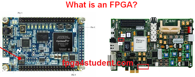
Thus, FPGAs are nothing, but logic blocks and interconnects that can be programmable by Hardware Description Languages (Verilog HDL/ VHDL) to perform different complex functions.
In fact, FPGAs can be used to implement almost any DSP algorithm. Some FPGAs also obtain embedded soft-core processors such as Xilinx's MicroBlaze, Altera's Nios II, etc. so that we can use C, C++, etc. to program the processor like what we do with a microcontroller. Besides, the soft processors can communicate with hardware accelerators to speed up complex DSP operations so that we can obtain a better flexible embedded system for niche applications.
Let's take a very basic example on how to use an FPGA. Let's assume that you are designing a 1-bit full adder and you already obtained the logic diagram of the adder as shown in the figure below.
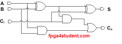 As mentioned above, there are necessary logic gates on FPGA such as XOR, AND and OR in order to implement the above adder on FPGA. To demonstrate the operation of the adder on FPGA, either Verilog or VHDL can be easily used to connect those gates together as shown in the logic diagram of the adder.
- An example Verilog code for the adder:
-- FPGA Project: What is an FPGA?
-- Verilog example code for Adder on FPGA
module fpga4student_adder(input A,B,Ci, output S,Co);
 wire tmp1,tmp2,tmp3;  //FPGA projects
 xor u1(tmp1,A,B);  // Verilog projects
 and u2(tmp2,A,B);
 and u3(tmp3,tmp1,Ci);
 or u4(Co,tmp2,tmp3);
 xor u5(S,tmp1,Ci);
 endmodule
- An example VHDL code for the adder:
-- FPGA projects: What is an FPGA?
-- VHDL example code for adder on FPGA
 library ieee;
 use ieee.std_logic_1164.all;
 entity fpga4student_Adder is
   port( A, B, Ci : in std_logic;
      S, Co : out std_logic);
 end fpga4student_Adder;
 architecture structural of fpga4student_Adder is
 signal tmp1, tmp2, tmp3: std_logic;
 begin
   tmp1 <= A xor B;
   tmp2 <= A and B;
   tmp3 <= tmp1 and Ci;
   Co <= tmp2 or tmp3;
   S <= tmp1 xor Ci;
 end structural;
The Verilog/ VHDL code for the adder simply does the "wiring" job by connecting the logic gates on FPGA together to be functional as a full adder. After verifying the code by simulation, we can synthesize, run the adder on FPGA and see how it works. For simulation, there are various available simulators that we can use, but for students, I would recommend you to use ModelSim of Mentor Graphics. You can see more simulators here. For FPGA synthesis and FPGA programming, you can use Quartus II for Altera's FPGA Boards and Xilinx ISE or Vivado for Xilinx's FPGA Boards.
As an FPGA designer for several years, here are five reasons why I love FPGA design:
As an FPGA designer for several years, here are five reasons why I love FPGA design:
1. Very fast on-chip (FPGA) demonstration
The top reason why I love FPGA design is that it is very fast to verify a design on FPGA. While ASICs could take several months only for tape-out and another latency for PCB design, everything is settled on FPGA and we just need to download the program file to FPGA using a specific FPGA programming tool and see how it works on FPGA. FPGA boards of Xilinx and Altera provide necessary IOs and additional support circuits such as LCD, single LEDs, 7-segment LEDs, communication ports (USB, UART, VGA, HDMI, PS2, FMC, etc.), ADCs, DACs, CODEC, etc. so that FPGA can easily communicate with other chips for the verification process.
2. Simple and fast design process on FPGA
Another great thing to say about FPGA is that the design process is pretty simple and really easy to learn. The design flow for ASICs is very complicated and time-consuming since it needs a lot of complex steps for designing, verification, and implementation. On the other hand, FPGA design process mostly avoids sophisticated and time-consuming steps like Floor-planing, Timing Analysis, Physical Implementation, etc. because FPGA is already a characterized and verified chip. Of course, when needed, FPGA vendors also provide necessary tools for floorplanning and timing analysis to enable users optimizing performance for niche very-demanding designs. In fact, FPGA design flow only takes several steps such as HDL design and coding, functional simulation, synthesis, timing or post-synthesis simulation if needed, and Place And Route. Furthermore, many FPGA design tools are free and very easy for users to learn and design. FPGA vendors provide free user guides and tutorials to facilitate user's learning process. It could take very short time for students to be familiar with FPGA design if they have a good background in digital logic design.
3. FPGA's programmability
The highlight feature of FPGA we obviously could not omit is its programmability. While ASICs or microcontrollers are fixed in term of hardware (it can be programmable at the software level), FPGAs can be programmable at the hardware level. We can program FPGAs to perform almost any digital complex functionality and reconfigure it to whatever we want in the future if needed. FPGAs can be programmed as a microprocessor, a microcontroller, DSPs, VGA controllers, digital filters, etc.
4. FPGA's high performance
Another superb feature in FPGA design is high performance. While processor-based ASICs or DSPs are sequential executed, FPGAs exploits the hardware parallelism to obtain a breakthrough performance for demanding designs. Thus, FPGAs provides faster implementations that processor-based ASICs could not match. The FPGA's parallelism can be effectively exploited to implement digital signal processing algorithms in order to speed up the processing time.
5. FPGA's flexibility
FPGAs are more and more flexible for designers to make their own applications. As mentioned above, FPGA vendors provide their own soft processors such as Xilinx's MicroBlaze, Altera's Nios II, etc. so that designers can be more flexible in design and programming process. Indeed, on FPGA, you can use the soft processors with the software-level-reconfigurable capability(C, C++, etc.) for low and average speed applications, and FPGA hardware accelerators with the hardware-level-reconfigurable capability(Verilog/ VHDL) for high-speed operations. Thus, designers can obtain a suitable embedded system which meets their design requirements. For example, when designing an embedded real-time tracking system, designers can use the soft processor for camera interface and FPGA hardware accelerators for tracking processing.
Verilog vs VHDL: Explain by Examples
What is FPGA Programming? FPGA vs Software programming
Recommended and affordable Xilinx FPGA boards for students
Recommended and affordable Altera FPGA boards for students
Verilog vs VHDL: Explain by Examples
What is FPGA Programming? FPGA vs Software programming
Recommended and affordable Xilinx FPGA boards for students
Recommended and affordable Altera FPGA boards for students
Recommended FPGA projects for students:
1. What is FPGA? How does FPGA work?
2. Basys 3 FPGA OV7670 Camera
3. How to load text file or image into FPGA
4. Image processing on FPGA using Verilog
5. License Plate Recognition on FPGA
6. Alarm Clock on FPGA using Verilog
7. Digital Clock on FPGA using VHDL
8. Simple Verilog code for debouncing buttons on FPGA
9. Traffic Light Controller on FPGA
10. Car Parking System on FPGA in Verilog
11. VHDL code for comparator on FPGA
12. Verilog code for Multiplier on FPGA
13. N-bit Ring Counter in VHDL on FPGA
14. Verilog implementation of Microcontroller on FPGA
15. Verilog Carry Look Ahead Multiplier on FPGA
16. VHDL Matrix Multiplication on FPGA Xilinx
17. Fixed Point Matrix Multiplication on FPGA using Verilog
18. Verilog Divider on FPGA
19. VHDL code for Microcontroller on FPGA
20. VHDL code for FIR Filter on FPGA
21. Verilog code for Digital logic components on FPGA
22. Delay Timer Implementation on FPGA using Verilog
23. Single-Cycle MIPS processor on FPGA using Verilog
24. FIFO Verilog Implementation on FPGA
25. FIFO VHDL Implementation on FPGA
26. Verilog D Flip Flop on FPGA
27. Comparator Design on FPGA using Verilog
28. D Flip Flop on FPGA using VHDL
29. Full Adder Design on FPGA using Verilog
30. Full Adder Design on FPGA using VHDL
31. Counters on FPGA with Verilog Testbench
32. RISC Processor Design on FPGA using Verilog
33. Verilog test bench for inout ports on FPGA
34. PWM Generator on FPGA using VHDL
35. Tic Tac Toe Game on FPGA using Verilog
36. VHDL code for ALU on FPGA
37. Verilog code for ALU on FPGA
38. Counter design on FPGA with VHDL test bench
39. Pipelined MIPS Processor on FPGA in Verilog (Part-1)
40. Pipelined MIPS Processor on FPGA in Verilog (Part-2)
41. Pipelined MIPS Processor on FPGA in Verilog (Part-3)
42. Verilog Decoder on FPGA
43. Verilog Multiplexers on FPGA
44. N-bit Adder Design on FPGA in Verilog
45. VHDL ALU on FPGA using N-bit Verilog Adder
46. VHDL Shifter on FPGA
47. Lookup Table VHDL example code on FPGA
48. Coprocessor VHDL Implementation on FPGA
49. Affordable Xilinx FPGA boards for beginners
50. Affordable Altera FPGA boards for beginners


No comments:
Post a Comment