

VHDL code for Matrix multiplication is presented. This VHDL project is aimed to develop and implement a synthesizable matrix multiplier core, which is able to perform matrix calculation for matrices with the size of 32x32.
Each component of the matrices is 16-bit unsigned integer. The core is implemented on Xilinx FPGA Spartan-6 XC6SLX45-CSG324-3. Both behavior and post-route verification are completed. The simulated result is accurately compared to Matlab implementation result.
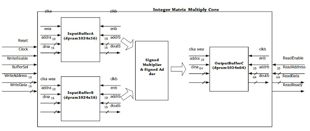
Block diagram of the design core
The design core is based on the reference design of matrix addition, which input and output buffers are generated by Xilinx Core Generator to save input and output data. The main work is the block to calculate matrix multiplication. Based on the theory of matrix multiplication, the matrix multiplication is done by the following equation:
To calculate cij , during the state of “stReadBufferAB”, we have to read out all 32 columns of row i and 32 the rows of column j, and do multiplication and accumulation like the equation. Furthermore, we add one more state “stSaveData” to the FSM of the reference core which is aimed to save the accumulated data before going to the next state of “stWriteBufferC”.
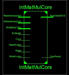
Block interface of the design core
VHDL top level code for the matrix multiplier:
 -- fpga4student.com FPGA projects, Verilog projects, VHDL projects
 -- VHDL project: VHDL code for matrix multiplcation
 library ieee;
 use ieee.std_logic_1164.all;
 use ieee.numeric_std.all;
 use IEEE.STD_LOGIC_UNSIGNED.ALL;
 -- Required entity declaration
 entity IntMatMulCore is
      port(
           Reset, Clock,      WriteEnable, BufferSel:      in std_logic;
           WriteAddress: in std_logic_vector (9 downto 0);
           WriteData:           in std_logic_vector (15 downto 0);
           ReadAddress:      in std_logic_vector (9 downto 0);
           ReadEnable:      in std_logic;
           ReadData:           out std_logic_vector (63 downto 0);
           DataReady:           out std_logic
      );
 end IntMatMulCore;
 architecture IntMatMulCore_arch of IntMatMulCore is
 -- fpga4student.com FPGA projects, Verilog projects, VHDL projects
 COMPONENT dpram1024x16
  PORT (
   clka : IN STD_LOGIC;
   wea : IN STD_LOGIC_VECTOR(0 DOWNTO 0);
   addra : IN STD_LOGIC_VECTOR(9 DOWNTO 0);
   dina : IN STD_LOGIC_VECTOR(15 DOWNTO 0);
   clkb : IN STD_LOGIC;
       enb : IN STD_LOGIC;
   addrb : IN STD_LOGIC_VECTOR(9 DOWNTO 0);
   doutb : OUT STD_LOGIC_VECTOR(15 DOWNTO 0)
  );
 END COMPONENT;
 -- fpga4student.com FPGA projects, Verilog projects, VHDL projects
 COMPONENT dpram1024x64
  PORT (
   clka : IN STD_LOGIC;
   wea : IN STD_LOGIC_VECTOR(0 DOWNTO 0);
   addra : IN STD_LOGIC_VECTOR(9 DOWNTO 0);
   dina : IN STD_LOGIC_VECTOR(63 DOWNTO 0);
   clkb : IN STD_LOGIC;
   enb : IN STD_LOGIC;
   addrb : IN STD_LOGIC_VECTOR(9 DOWNTO 0);
   doutb : OUT STD_LOGIC_VECTOR(63 DOWNTO 0)
  );
 END COMPONENT;
 -- fpga4student.com FPGA projects, Verilog projects, VHDL projects
 type     stateType is (stIdle, stWriteBufferA, stWriteBufferB, stReadBufferAB, stSaveData, stWriteBufferC, stComplete);
 signal presState: stateType;
 signal nextState: stateType;
 signal iReadEnableAB, iCountReset,iCountEnable, iCountEnableAB,iCountResetAB: std_logic;
 signal iWriteEnableA, iWriteEnableB, iWriteEnableC: std_logic_vector(0 downto 0);
 signal iReadDataA, iReadDataB: std_logic_vector (15 downto 0);
 signal iWriteDataC: std_logic_vector (63 downto 0);
 signal iCount, iReadAddrA, iReadAddrB,iRowA : unsigned(9 downto 0);
 signal CountAT,CountBT:unsigned(9 downto 0);
 signal iColB:unsigned(19 downto 0);
 signal irow,icol,iCountA,iCountB: unsigned(4 downto 0);
 signal iCountEnableAB_d1,iCountEnableAB_d2,iCountEnableAB_d3: std_logic;
 begin
      --Write Enable for RAM A
      iWriteEnableA(0) <= WriteEnable and BufferSel;
      --Write Enable for RAM B
      iWriteEnableB(0) <= WriteEnable and (not BufferSel);
 -- fpga4student.com FPGA projects, Verilog projects, VHDL projects
      --Input Buffer A Instance
           InputBufferA : dpram1024x16
           PORT MAP (
                clka => Clock,
                wea  => iWriteEnableA,
                addra => WriteAddress,
                dina => WriteData,
                clkb      => Clock,
                enb     => iReadEnableAB,
                addrb => std_logic_vector(iReadAddrA),
                doutb => iReadDataA
           );
 -- fpga4student.com FPGA projects, Verilog projects, VHDL projects
      InputBufferB : dpram1024x16
           PORT MAP (
                clka => Clock,
                wea  => iWriteEnableB,
                addra => WriteAddress,
                dina => WriteData,
                clkb      => Clock,
                enb     => iReadEnableAB,
                addrb => std_logic_vector(iReadAddrB),
                doutb => iReadDataB
           );
 -- fpga4student.com FPGA projects, Verilog projects, VHDL projects
      OutputBufferC : dpram1024x64
           PORT MAP (
                clka      => Clock,
                wea      => iWriteEnableC,
                addra => std_logic_vector(iCount),
                dina      => iWriteDataC,
                clkb      => Clock,
                enb      => ReadEnable,
                addrb => ReadAddress,
                doutb => ReadData
           );
      process(Clock,Reset)
      begin
      if(rising_edge(Clock)) then
      if(Reset='1') then
      iCountEnableAB_d1 <= '0';
      iCountEnableAB_d2 <= '0';
      else
      iCountEnableAB_d1 <= iCountEnable;
      iCountEnableAB_d2 <= iCountEnableAB_d1;
      end if;
      end if;
      end process;
      iCountEnableAB_d3 <= (not iCountEnableAB_d2) AND iCountEnableAB_d1 ;
 -- fpga4student.com FPGA projects, Verilog projects, VHDL projects
      process (Clock)
      begin
           if rising_edge (Clock) then
                if(Reset='1') then
                     iWriteDataC <= (others => '0');
                elsif(iWriteEnableC(0)='1') then
                     iWriteDataC <= (others => '0');
                elsif(iCountEnableAB_d3='1') then
                     iWriteDataC <= (others => '0');
                elsif(iReadEnableAB='1') then
                     iWriteDataC <= iWriteDataC + std_logic_vector(signed(iReadDataA(15)&iReadDataA)*signed(iReadDataB(15)&iReadDataB));
                end if;
           end if;
      end process;
 -- fpga4student.com FPGA projects, Verilog projects, VHDL projects
       process (Clock)
      begin
           if rising_edge (Clock) then
                if Reset = '1' then
                     presState <= stIdle;
                     iCountA <= (others=>'0');
                     iCountB <= (others=>'0');
                else
                     presState <= nextState;
                     if iCountResetAB = '1' then
                          iCountA <= (others=>'0');
                          iCountB <= (others=>'0');
                     elsif iCountEnableAB = '1' then
                          iCountA <= iCountA + 1;
                          iCountB <= iCountB + 1;
                     end if;
                end if;
                if iCountReset = '1' then
                     iCount <= (others=>'0');
                elsif iCountEnable = '1' then
                     iCount <= iCount + 1;
                end if;
           end if;
      end process;
      iRowA <= iCount srl 5;
      iColB <= ("0000000000"&iCount) - iRowA*32;
      irow <= iRowA(4 downto 0);
      icol <= iColB(4 downto 0);
      CountAT <= "00000"&iCountA;
      CountBT <= "00000"&iCountB;
      iReadAddrA <= (iRowA sll 5)+CountAT;
      iReadAddrB <= (CountBT sll 5)+ iColB(9 downto 0);
 -- fpga4student.com FPGA projects, Verilog projects, VHDL projects
      process (presState, WriteEnable, BufferSel, iCount, iCountA, iCountB)
      begin
           -- signal defaults
           iCountResetAB <= '0';
           iCountReset <= '0';
           iCountEnable <= '1';
           iReadEnableAB <= '0';
           iWriteEnableC(0) <= '0';
           Dataready <= '0';
           iCountEnableAB <= '0';
           case presState is
                when stIdle =>
                     if (WriteEnable = '1' and BufferSel = '1') then
                          nextState <= stWriteBufferA;
                     else
                          iCountReset <= '1';
                          nextState <= stIdle;
                     end if;
                when stWriteBufferA =>
                     if iCount = x"3FF" then
                          report "Writing A";
                          iCountReset <= '1';
                          nextState <= stWriteBufferB;
                      else
                          nextState <= stWriteBufferA;
                     end if;
                when stWriteBufferB =>
                     report "Writing B";
                     if iCount = x"3FF" then
                          iCountReset <= '1';
                          nextState <= stReadBufferAB;
                      else
                          nextState <= stWriteBufferB;
                     end if;
                when stReadBufferAB =>
                     iReadEnableAB <= '1';
                     iCountEnable <= '0';
                     report "CalculatingAB";
                     if iCountA = x"1F" and iCountB = x"1F" then
                          nextState <= stSaveData;
                          report "Calculating";
                          iCountEnableAB <= '0';
                          iCountResetAB <= '1';
                     else
                          nextState <= stReadBufferAB;
                          iCountEnableAB <= '1';
                          iCountResetAB <= '0';
                     end if;
                when stSaveData =>
                     iReadEnableAB <= '1';
                     iCountEnable <= '0';
                     nextState <= stWriteBufferC;
                when stWriteBufferC =>
                     iWriteEnableC(0) <= '1';
                     report "finish 1 component";
                     if iCount = x"3FF" then
                          iCountReset <= '1';
                          nextState <= stComplete;
                      else
                          nextState <= stReadBufferAB;
                     end if;
                when stComplete =>
                     DataReady <= '1';
                     nextState <= stIdle;
           end case;
      end process;
 end IntMatMulCore_arch;
Below is the testbench code to read matrix inputs from text files and write the result to an output text file:
-- VHDL project: VHDL code for matrix multiplication
-- fpga4student.com FPGA projects, Verilog projects, VHDL projects
-- Testbench VHDL code for matrix multiplication
 library ieee;
 use ieee.std_logic_1164.all;
 use ieee.std_logic_textio.all;
 use ieee.numeric_std.all;
 use std.textio.all;
 entity tb_IntMatMultCore is
 end tb_IntMatMultCore;
 architecture behavior of tb_IntMatMultCore is
 component IntMatMulCore
      port(
           Reset, Clock,      WriteEnable, BufferSel:      in std_logic;
           WriteAddress: in std_logic_vector (9 downto 0);
           WriteData:           in std_logic_vector (15 downto 0);
           ReadAddress:      in std_logic_vector (9 downto 0);
           ReadEnable:      in std_logic;
           ReadData:           out std_logic_vector (63 downto 0);
           DataReady:           out std_logic
      );
 end component;
 signal tb_Reset : std_logic := '0';
 signal tb_Clock : std_logic := '0';
 signal tb_BufferSel : std_logic := '0';
 signal tb_WriteEnable : std_logic := '0';
 signal tb_WriteAddress : std_logic_vector(9 downto 0) := (others => '0');
 signal tb_WriteData : std_logic_vector(15 downto 0) := (others => '0');
 signal tb_ReadEnable : std_logic := '0';
 signal tb_ReadAddress : std_logic_vector(9 downto 0) := (others => '0');
 signal tb_DataReady : std_logic;
 signal tb_ReadData : std_logic_vector(63 downto 0);
 -- Clock period definitions
 constant period : time := 100 ns;
 begin
 -- fpga4student.com FPGA projects, Verilog projects, VHDL projects
      -- Instantiate the Unit Under Test (UUT)
      uut: IntMatMulCore
           PORT MAP (
                Reset                    => tb_Reset,
                Clock                    => tb_Clock,
                WriteEnable          => tb_WriteEnable,
                BufferSel          => tb_BufferSel,
                WriteAddress     => tb_WriteAddress,
                WriteData          => tb_WriteData,
                ReadEnable          => tb_ReadEnable,
                ReadAddress          => tb_ReadAddress,
                ReadData               => tb_ReadData,
                DataReady          => tb_DataReady
    );
  -- Test Bench Statements
      process is
      begin
           --while now <= 10000000000000 * period loop
                tb_Clock <= '0';
                wait for period/2;
                tb_Clock <= '1';
                wait for period/2;
           --end loop;
           --wait;
      end process;
      process is
      begin
           tb_Reset <= '1';
           wait for 10*period;
           tb_Reset <= '0';
           wait;
      end process;
      writingA: process is
           file FIA: TEXT open READ_MODE is "InputA.txt";  -- the input file must have 17 rows
           file FIB: TEXT open READ_MODE is "InputB.txt";  -- the input file must have 17 rows
           variable L: LINE;
           variable tb_MatrixData: std_logic_vector(15 downto 0);
      begin
           tb_WriteEnable <= '0';
           tb_BufferSel <= '1';
           tb_WriteAddress <= "11"&x"FF";
           wait for 20*period;
           READLINE(FIA, L);
           while not ENDFILE(FIA) loop
                READLINE(FIA, L);
                HREAD(L, tb_MatrixData);
                wait until falling_edge(tb_Clock);
                tb_WriteAddress <= std_logic_vector(unsigned(tb_WriteAddress)+1);
                tb_BufferSel <= '1';
                tb_WriteEnable <= '1';
                tb_WriteData <=tb_MatrixData;
           end loop;
           READLINE(FIB, L);
           while not ENDFILE(FIB) loop
                READLINE(FIB, L);
                HREAD(L, tb_MatrixData);
                wait until falling_edge(tb_Clock);
                tb_WriteAddress <= std_logic_vector(unsigned(tb_WriteAddress)+1);
                tb_BufferSel <= '0';
                tb_WriteEnable <= '1';
                tb_WriteData <=tb_MatrixData;
           end loop;
           wait for period;
           tb_WriteEnable <= '0';
           wait;
      end process;
 -- fpga4student.com FPGA projects, Verilog projects, VHDL projects
      reading: process is
           file FO: TEXT open WRITE_MODE is "OutputMultC.txt";
           file FI: TEXT open READ_MODE is "OutputMultC_matlab.txt";
           variable L, Lm: LINE;
           variable v_ReadDatam: std_logic_vector(63 downto 0);
           variable v_OK: boolean;
      begin
           tb_ReadEnable <= '0';
           tb_ReadAddress <=(others =>'0');
           ---wait for Mul done
           wait until rising_edge(tb_DataReady);
           wait until falling_edge(tb_DataReady);
           READLINE(FI, Lm);
           Write(L, STRING'("OutputMultC"));
           WRITELINE(FO, L);
           tb_ReadEnable<= '1' ;
           while not ENDFILE(FI) loop
                wait until rising_edge(tb_Clock);
                wait for 20 ns;
                READLINE(FI, Lm);
                HREAD(Lm, v_ReadDatam);
                if v_ReadDatam = tb_ReadData then
                     v_OK :=True;
                     report "Matched";
                else
                     v_OK :=False;
                end if;
                HWRITE(L, '0'& tb_ReadData, Left, 10);
                WRITE(L, v_OK, Right, 10);
                WRITELINE(FO, L);
                tb_ReadAddress <= std_logic_vector(unsigned(tb_ReadAddress)+1);
           end loop;
           tb_ReadEnable <= '0';
           assert false report "Simulation Finished" severity failure; -- to stop simulation
           wait;
      end process;
 end;
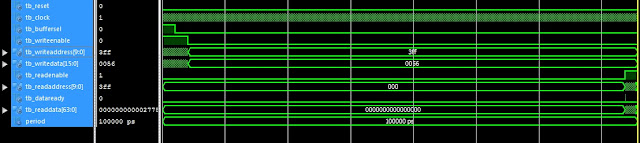
Behavior Simulation for the matrix multiplication design
After finishing the design of the multiplier core, we carry out the behavior simulation for the core. The testbench is reading input A and B, then produce output C and then compare with Matlab result. If the result is 100% compared to Matlab, data in output file “OutputMultC.txt” will be “true”. Otherwise, it will be false.
Behavior simulation waveform
After 34816 clock cycles, the matrix multiplication for the matrix with size 32x32 is completed and the signal “dataready” is asserted high. It is reasonable because it would take 32 cycles to calculate each matrix component of the output matrix C. There are also 2 cycles which are saving data and writing data to buffer C for each matrix component. Thus, there are 34 clock cycles being used to calculate one component of matrix C. The size of matrix C is 32x32, then we have the matrix multiplication time is 32x32x34 = 34816 cycles.
The behavior simulation result is correctly compared to Matlab. In fact, the output file “OutputMultC.txt” is all “true”. We also check the memory content of the buffer output and the results are of course similar to Matlab calculation.
Post-route simulation
To perform post-route simulation, we synthesize and get the post translate netlist to be simulated. The synthesis result indicates that the maximum frequency of the clock used for this design is 120.757MHz. It means that the minimum period of the clock is 8.281ns. Thus, the minimum multiplication time for the 32x32 matrixes is 34816x8.281ns = 288.311 us.
The post-route simulation result is accurately similar to the Matlab result and the behavior simulation. Indeed, the output file “OutputMultC.txt” is all “true” as our expectation.
In this project, the matrix multiplication for the matrixes with 32x32 16-bit unsigned integers is implemented on FPGA Spartan6 of Xilinx. The minimum multiplication time for the matrix of 32x32 is 288.311 us.
Recommended VHDL projects:
1. What is an FPGA? How VHDL works on FPGA
2. VHDL code for FIFO memory
3. VHDL code for FIR Filter
4. VHDL code for 8-bit Microcontroller
5. VHDL code for Matrix Multiplication
6. VHDL code for Switch Tail Ring Counter
7. VHDL code for digital alarm clock on FPGA
8. VHDL code for 8-bit Comparator
9. How to load a text file into FPGA using VHDL
10. VHDL code for D Flip Flop
11. VHDL code for Full Adder
12. PWM Generator in VHDL with Variable Duty Cycle
13. VHDL code for ALU
14. VHDL code for counters with testbench
15. VHDL code for 16-bit ALU
16. Shifter Design in VHDL
17. Non-linear Lookup Table Implementation in VHDL
18. Cryptographic Coprocessor Design in VHDL
19. Verilog vs VHDL: Explain by Examples
20. VHDL Code for Clock Divider on FPGA
21. How to generate a clock enable signal instead of creating another clock domain
22. VHDL code for debouncing buttons on FPGA
23. VHDL code for Traffic light controller
24. VHDL code for a simple 2-bit comparator
25. VHDL code for a single-port RAM
22. VHDL code for debouncing buttons on FPGA
23. VHDL code for Traffic light controller
24. VHDL code for a simple 2-bit comparator
25. VHDL code for a single-port RAM
26. VHDL code for Car Parking System using FSM
27. VHDL coding vs Software Programming


Hi!
ReplyDeleteCan I implement this project with Vivado 2015.4 on board Basys 3. I tried to do this, but Vivado 2015.4 doesn't read/take these files (InputBufferA - dpram1024x16, InputBufferB - dpram1024x16 and OutputBufferC - dpram1024x64)
Or I'll have to create them and throw in a folder "sources".
Can you help me? I would be happy for the answer.
You have to use Xilinx Generator to generate that memory. Then include it into the project.
ReplyDeleteCan this code be used for FPGA Model DE2i - 150
ReplyDeleteIt can be possible but you need to replace the Block RAM IP of Xilinx by that of Quartus Altera.
Deletethis bullshit doesn't work :D
ReplyDeleteHi, I am getting an error with Read command. From Input A file. Do I have to import any i/o packages?
ReplyDeleteCan someone present containage of inputA, inputB, outputC and OutputC Matlab files please
ReplyDelete